Electronic emitter and production method thereof, electron source and visual display unit

一种电子发射、制造方法的技术,应用在图像/图形显示管、电极系统制造、放电管/灯的制造等方向,能够解决电子漫射、表面粗糙度大、制造出电子发射器件等问题,达到性能卓越的效果

Inactive Publication Date: 2009-04-29
CANON KK
View PDF5 Cites 4 Cited by
  • Summary
  • Abstract
  • Description
  • Claims
  • Application Information

AI Technical Summary

Problems solved by technology

[0006] However, it is difficult to manufacture diamond with a uniform film thickness over a large area, making it difficult to manufacture electron-emitting devices uniformly over a large area
Also, since the surface roughness is large, the emitted electrons are diffused, making it difficult to display high-definition images

Method used


Image

  • Electronic emitter and production method thereof, electron source and visual display unit
  • Electronic emitter and production method thereof, electron source and visual display unit
  • Electronic emitter and production method thereof, electron source and visual display unit

Examples


no. 1 example

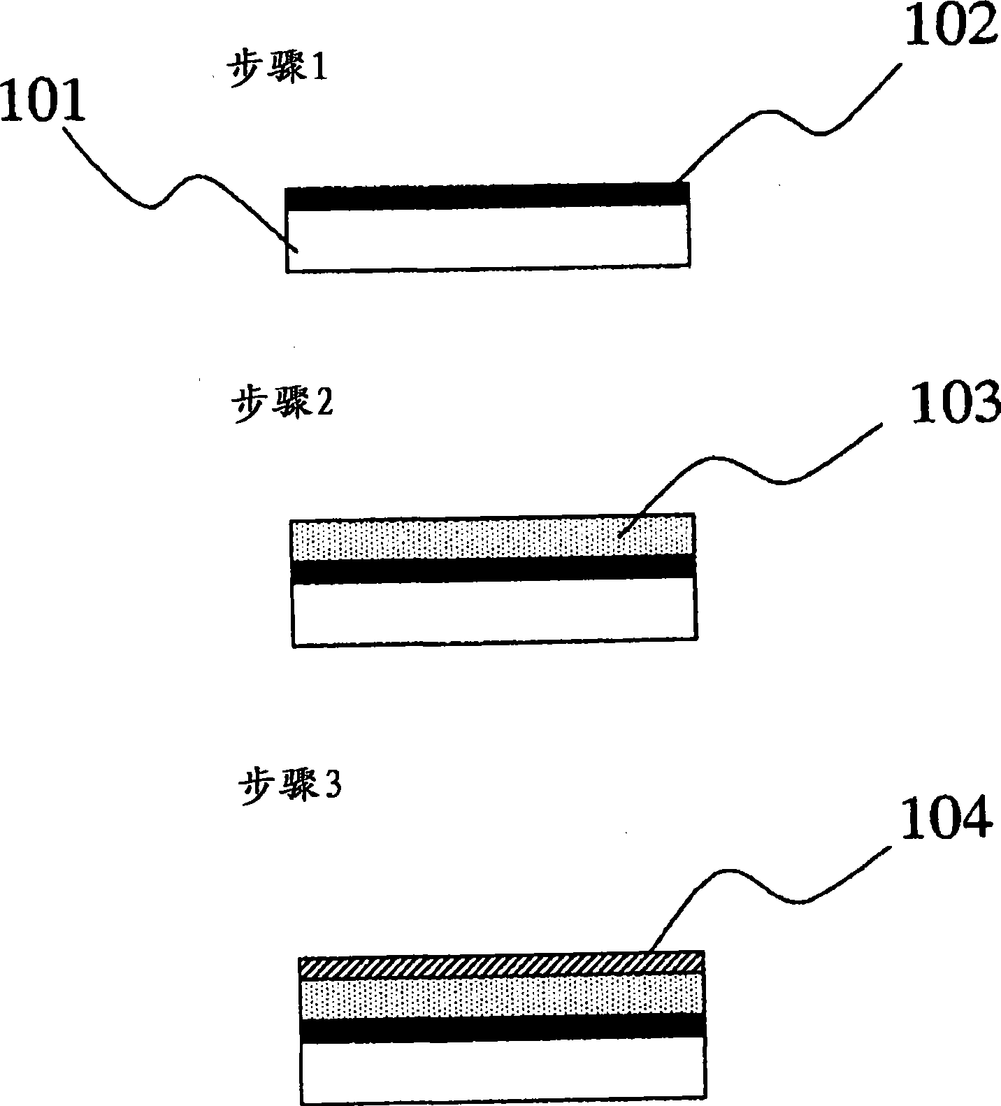
[0085] In the following, reference will be made to figure 1 The steps of manufacturing the electron emission film according to this example are described in detail.

[0086] (step 1)

[0087] First, quartz glass as the substrate 101 was sufficiently cleaned, and a Pt film as the cathode electrode 102 was formed on the substrate 101 with a thickness of 200 nm by the sputtering method.

[0088] (step 2)

[0089] A diamond-like carbon film containing Pt was formed as the electron emission film 103 on the cathode electrode 102 by using a co-sputtering method. The film thickness was about 30 nm, and the Pt density was about 20%.

[0090] (step 3)

[0091] The surface termination treatment was performed under the following conditions to form the hydrogen terminated surface 104 .

[0092] Process gas: CH 4 50 sccm

[0093] Pressure: 0.25Pa

[0094] ECR plasma power: 300W

[0095] Grid bias: -80V

[0096] Substrate Bias: +40V

[0097] Processing time: 30 seconds

[0098] ...

no. 2 example

[0101] In the following, reference will be made to figure 1 The steps of manufacturing the electron emission film according to this example are described in detail.

[0102] (step 1)

[0103] First, quartz glass as the substrate 101 was sufficiently cleaned, and a Pt film as the cathode electrode 102 was formed on the substrate 101 with a thickness of 200 nm by the sputtering method.

[0104] (step 2)

[0105] A Co-containing diamond-like carbon film was formed as the electron emission film 103 on the cathode electrode 102 by using a co-sputtering method. The film thickness was about 30 nm, and the Co density was about 20%.

[0106] (step 3)

[0107] The surface termination treatment was performed under the following conditions to form the hydrogen terminated surface 104 .

[0108] Process gas: CH 4 20 sccm

[0109] h 2 30 sccm

[0110] Pressure: 0.25Pa

[0111] ECR plasma power: 400W

[0112] Grid bias: 0V

[0113] Substrate Bias: +40V

[0114] Processing time:...

no. 3 example

[0118] In the following, reference will be made to figure 1 The steps of manufacturing the electron emission film according to this example are described in detail.

[0119] (step 1)

[0120]First, quartz glass as the substrate 101 was sufficiently cleaned, and a Pt film with a thickness of 200 nm as the cathode electrode 102 was formed on the substrate 101 by the sputtering method.

[0121] (step 2)

[0122] A carbon film is formed on the cathode electrode 102 by using a filament CVD (filament CVD) method. Thereafter, by implanting 1 atm% Co into the diamond-like carbon film by an ion implantation method, an electron emission film was formed. The film thickness was about 30 nm.

[0123] (step 3)

[0124] The surface termination treatment was performed under the following conditions to form the hydrogen terminated surface 104 .

[0125] Process gas: C 2 h 4 30 sccm

[0126] h 2 20 sccm

[0127] Pressure: 0.25Pa

[0128] ECR plasma power: 300W

[0129] Grid bias:...


PUM


Abstract

A manufacturing method of an electron-emitting device including the steps of: preparing a base substrate provided with an insulating or semi-conducting layer in advance and exposing the layer to an atmosphere which contains neutral radical containing hydrogen. It is preferable that the insulating or semi-conducting layer contains metal particles; the insulating or semi-conducting layer is a film containing carbon as a main component; the neutral radical containing hydrogen contains any of H., CH3., C2H5., and C2H. or mixture gas thereof; compared with a density of a charged particle in the atmosphere, a density of the neutral radical containing hydrogen in the atmosphere is more than 1,000 times; and a step of exposing the insulating or semi-conducting layer to the atmosphere is a step of making a hydrogen termination by using a plasma apparatus provided with a bias grid.

Description

technical field [0001] The present invention relates to a method of manufacturing an electron-emitting device, an electron-emitting device, an electron source including the electron-emitting device, and an image display device including the electron source. Background technique [0002] Among the electron-emitting devices, there are field emission type (FE type), surface conduction type, and the like. [0003] In the FE type electron emission device, electrons are drawn from the cathode electrode (or the electron emission film) into a vacuum by applying a voltage between the cathode electrode (and the electron emission film disposed on the cathode electrode) and the gate electrode. Therefore, the operating electric field mainly depends on the work function of the cathode electrode (electron emission film) to be used, its shape, and the like. In general, it is necessary to select a cathode electrode (electron emission film) having a small work function. [0004] Diamond who...

Claims


Application Information

Patent Timeline
Patent Type & Authority Applications(China)
IPC IPC(8): H01J9/02H01J29/04H01J1/30H01J1/316H01J31/12
CPCH01J2329/0444H01J2201/30453H01J31/127H01J9/025
Inventor 寺本洋二藤原良治西村三千代野村和司村上俊介
Owner CANON KK
Why Eureka
Try Eureka