

High-efficient erasing and writing flash memory in grating
A split gate and flash memory technology, which is applied in the direction of electrical components, transistors, and electric solid-state devices, can solve the problem of device programming voltage reduction, achieve the effect of reducing erasing voltage, facilitating programming voltage, and increasing device density
- Summary
- Abstract
- Description
- Claims
- Application Information
AI Technical Summary
Problems solved by technology
Method used
Image

Examples
Embodiment Construction
[0024] In order to better understand the technical content of the present invention, specific embodiments are given together with the attached drawings for description as follows.
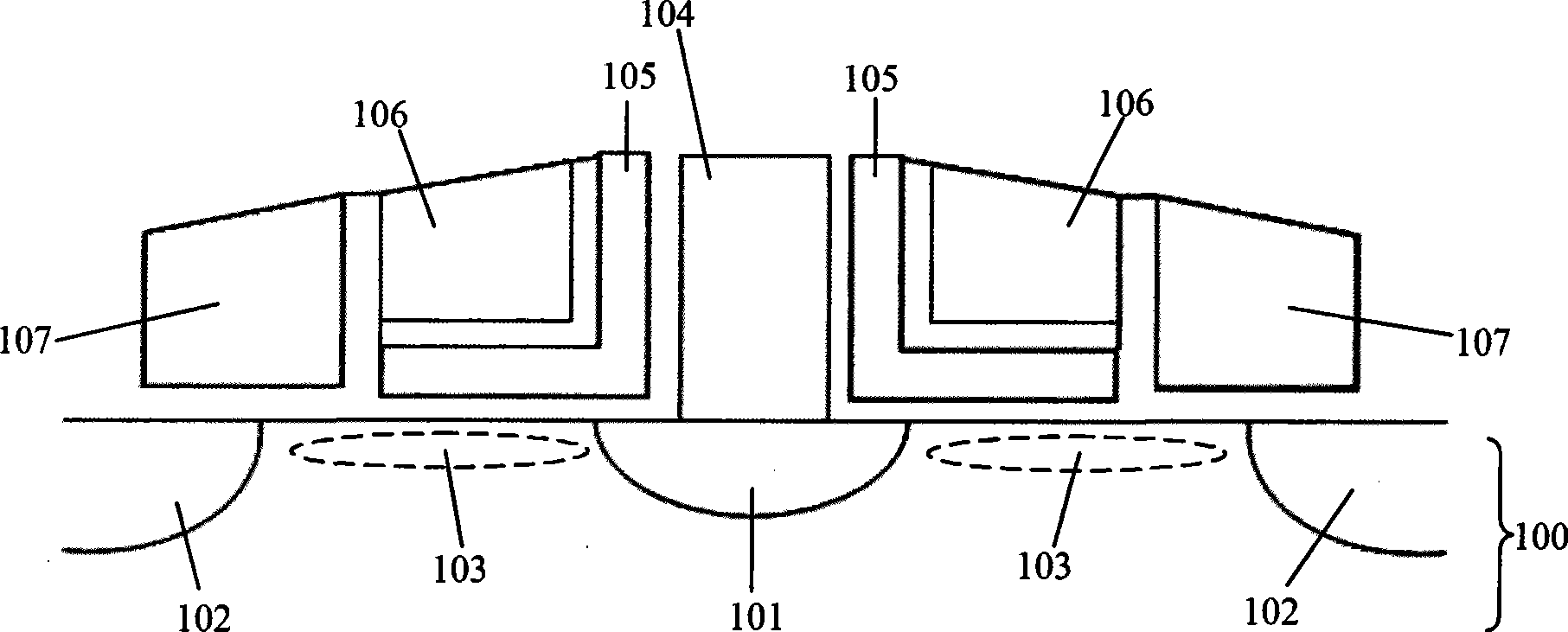
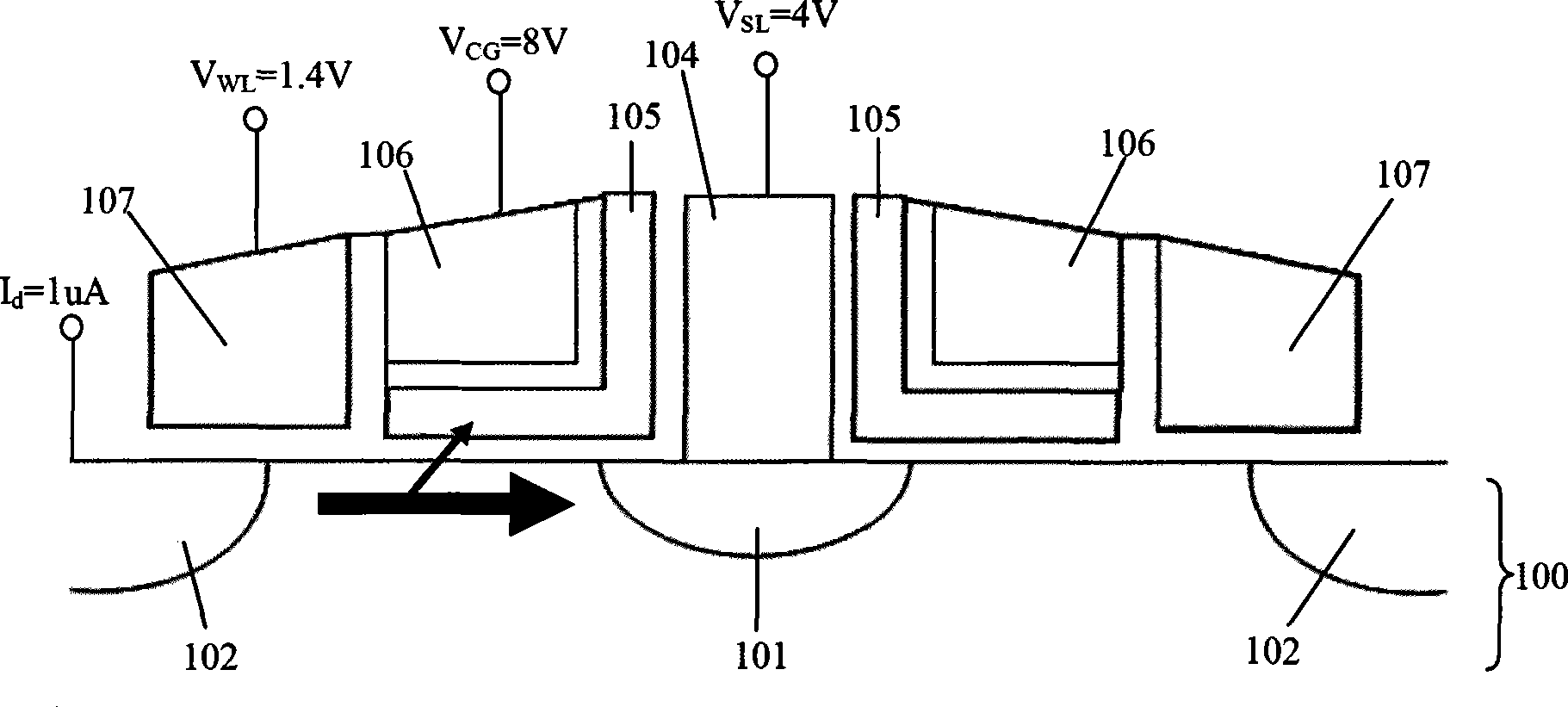
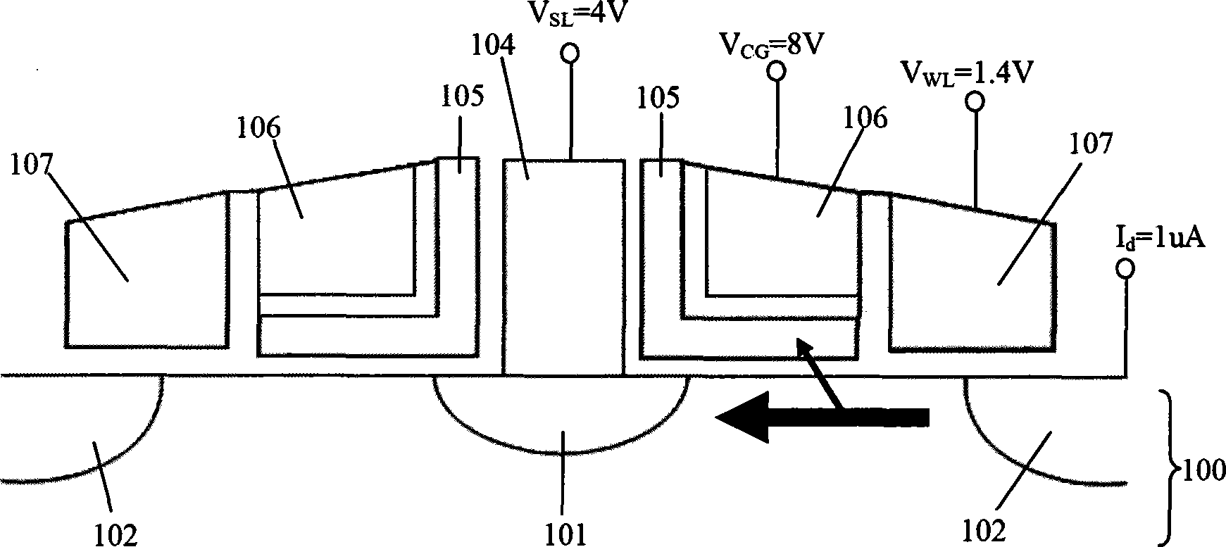
[0025] The invention proposes a high-efficiency erasable and rewritable split-gate flash memory, the programming voltage of which can be further reduced, thereby increasing device density. The invention provides a novel split-gate flash memory (Enhanced Program and Erase Split-gate Flash Memory) with high efficiency erasing and writing. It adopts a sidewall polysilicon layer as a storage area, injects charges into the sidewall polysilicon layer through hot electron injection, and then affects the channel of the transistor. channel current. In this way, the presence or absence of charge storage in the sidewall polysilicon layer can be sensed by the change in the channel current of the transistor. The state of whether the sidewall polysilicon layer has charge storage can be used to distinguish and s...
PUM
 Abstract
Description
Claims
Application Information