Trench gate SOI LIGBT device

A trench gate and device technology, applied in the field of semiconductor power devices, can solve problems such as prone to latch-up effect, LIGBT loses gate control ability, device failure, etc., and achieves the effects of preventing injection, avoiding opening, and reducing electric field strength

Inactive Publication Date: 2009-04-29
UNIV OF ELECTRONICS SCI & TECH OF CHINA
View PDF0 Cites 23 Cited by
  • Summary
  • Abstract
  • Description
  • Claims
  • Application Information

AI Technical Summary

Problems solved by technology

Compared with LDMOS, LIGBT has an anode P + Zone 4, P + Region 4 and N-type buffer layer 3, N-type drift region 6, P-type channel region 14 and N + Region 11 ...

Method used


Image

  • Trench gate SOI LIGBT device
  • Trench gate SOI LIGBT device
  • Trench gate SOI LIGBT device

Examples


Embodiment 1

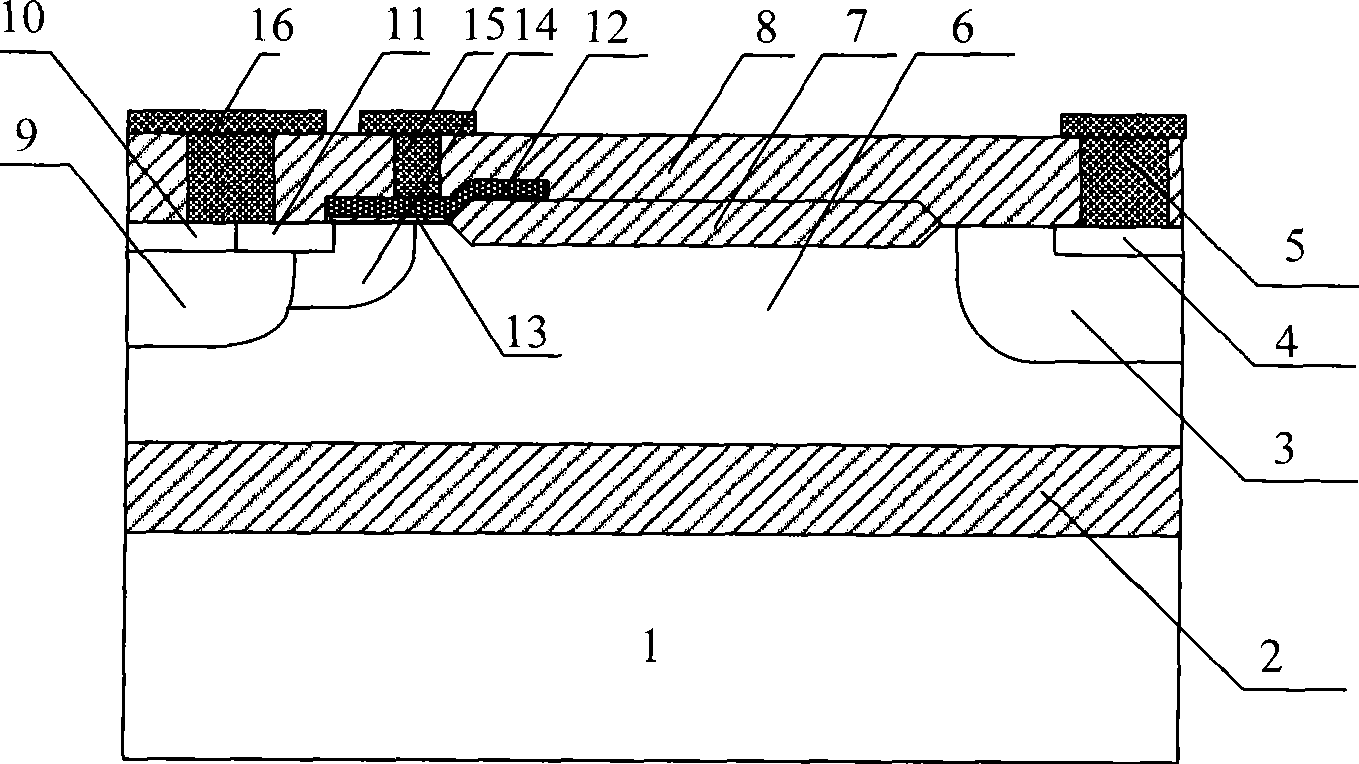
[0019] see figure 2 . Among them, the anode P + Region 4 is connected to anode metal 5, the concentration of P-type region 9 is higher than that of P-type channel region 14, and P + District 10 and N + Region 11 is in contact with cathode metal 16 . N + The region 11 is connected to the polysilicon trench gate 12 through the gate oxide layer of the LIGBT device, and the polysilicon trench gate 12 is connected to the polysilicon trench gate metal 15 .

Embodiment 2

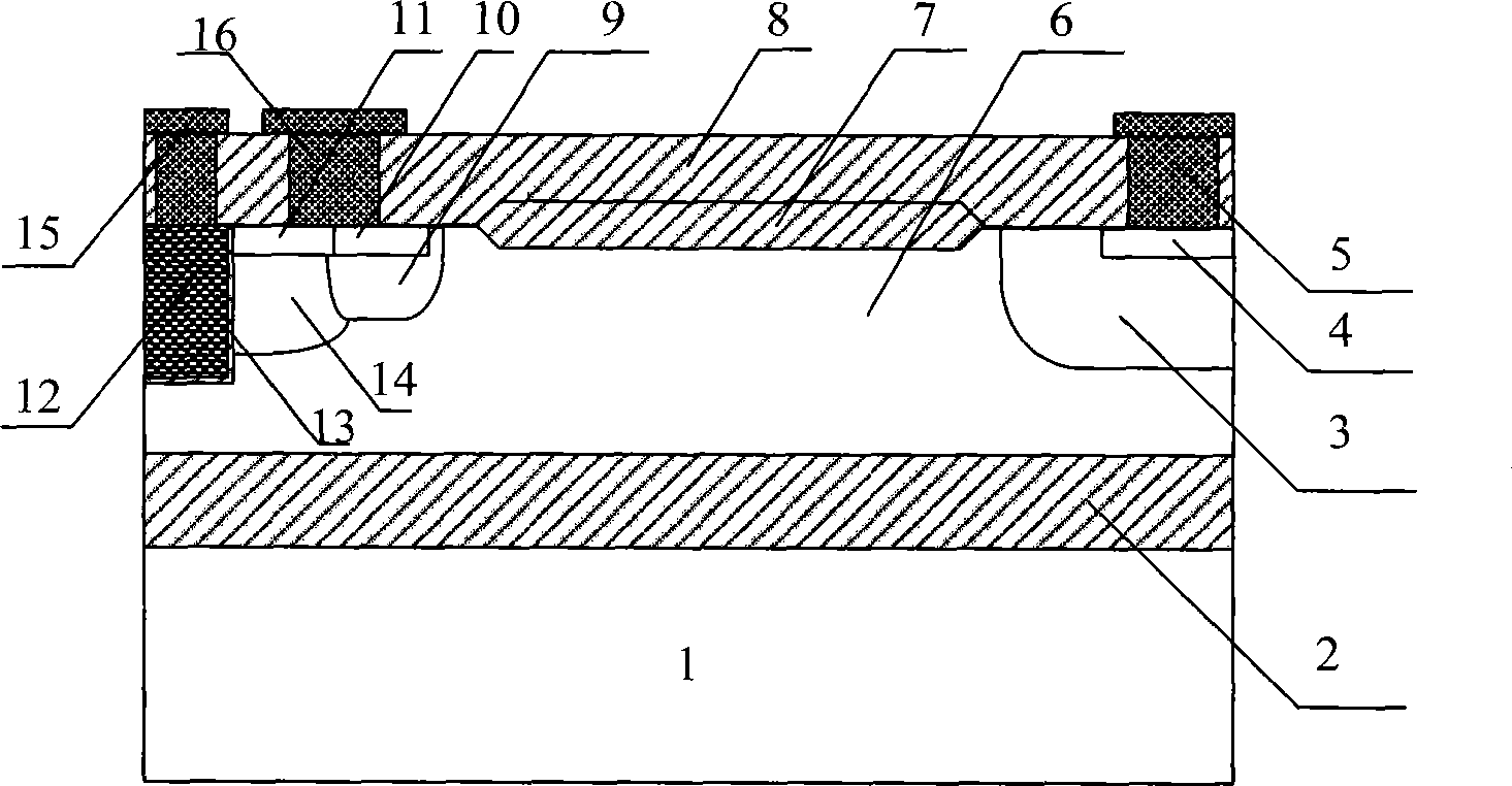
[0021] see image 3 . The difference between this embodiment and Embodiment 1 is that the polysilicon trench gate 12 of this embodiment is in contact with the buried oxide layer 2, and by means of the JFET effect, the depletion of the N-type drift region 6 under the P-type channel region 14 is enhanced to further reduce the The electric field strength near the gate oxide layer 13 is increased.

Embodiment 3

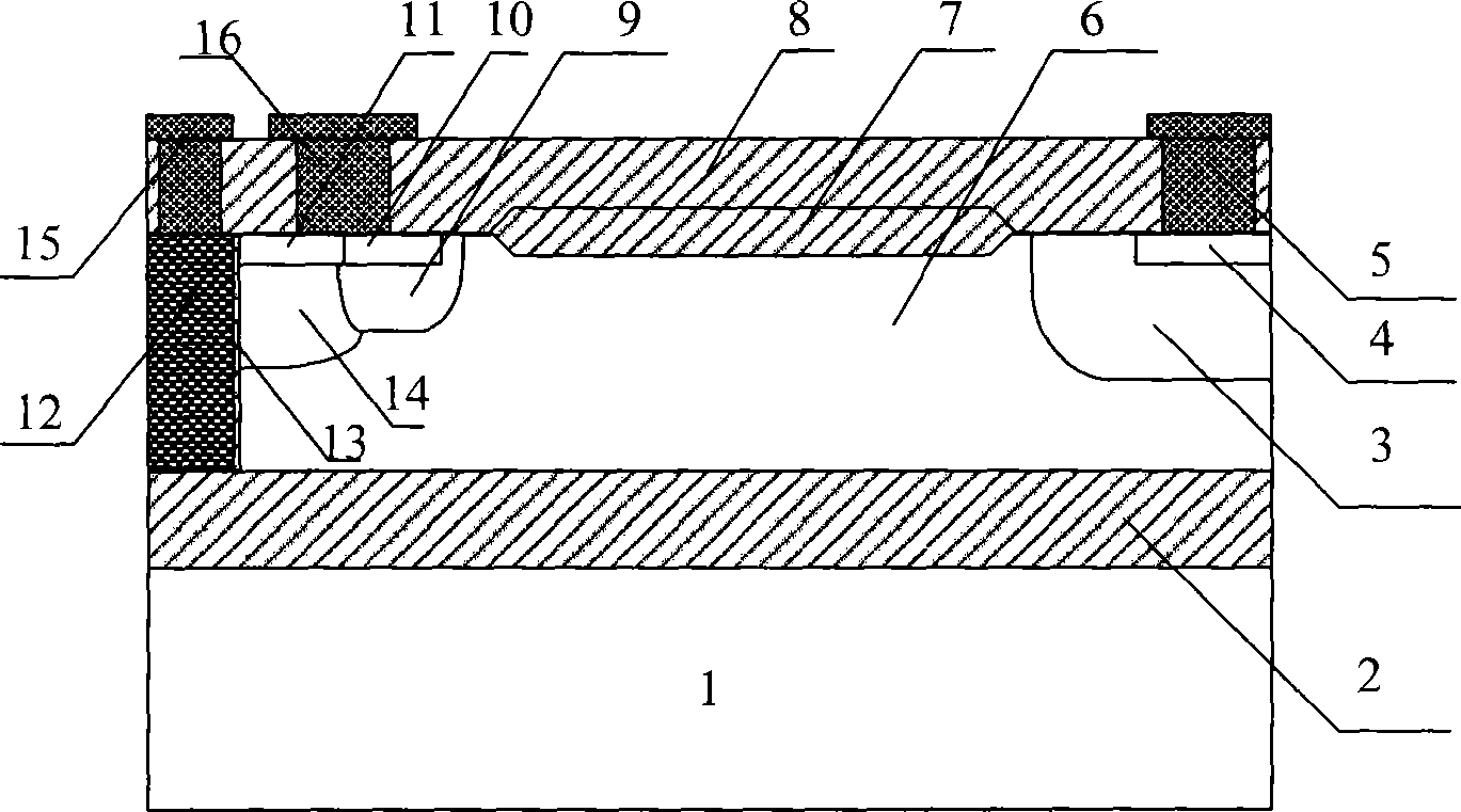
[0023] see Figure 4 . In this embodiment, the P-type region 9 is formed simultaneously with the P-type channel region 14, thereby saving the number of mask plates and reducing process complexity.


PUM


Abstract

The invention discloses a groove-gate SOI LIGBT device, and relates to semiconductor power device technologies. The groove-gate SOI LIGBT device comprises a substrate, a buried oxide layer, an N-type buffer layer, an anode P<+> region, an anode metal, an N-type drift region, a field oxide layer, a front metal dielectric layer, a P<+> region, an N<+> region, a polysilicon groove gate, an LIGBT device gate oxide layer, a P-type channel region, a polysilicon groove-gate metal and a cathode metal, the cathode metal is connected with the P<+> region and the N<+> region, and the P<+> region 10 is arranged between the N<+>region 11 and the anode P<+> region 4. The groove-gate SOI LIGBT device reduces the electric field intensity around the gate oxide layer, prevents a hot carrier from being implanted into the gate oxide, and improves the reliability of the device.

Description

technical field [0001] The invention relates to semiconductor power device technology. Background technique [0002] Lateral Insulated-Gate Bipolar Transistor LIGBT (Lateral Insulated-Gate Bipolar Transistor) is often used in the output stage of high-voltage power drive integrated circuits to improve the withstand voltage and conduction of lateral double-diffused metal-oxide-semiconductor field-effect transistors LDMOS (Lateral Double-diffusedMOSFET) The contradiction between the resistance. With its ideal dielectric isolation performance and relatively simple dielectric isolation process, SOI technology makes SOI devices have the advantages of small parasitic effects, fast speed, low power consumption, high integration, and strong radiation resistance. The integrated LIGBT device based on SOI technology, due to the complete dielectric isolation between the active device and the material substrate and other high and low voltage devices, is conducive to avoiding the latch-up...

Claims


Application Information

Patent Timeline
IPC IPC(8): H01L29/739H01L29/06
Inventor 乔明罗波杨帆刘新新张波
Owner UNIV OF ELECTRONICS SCI & TECH OF CHINA
Why Eureka
Try Eureka