Transient voltage suppressor manufactured in silicon on oxide (soi) layer

A technology of transient voltage suppression and silicon-on-insulator, which is applied in the field of circuit structure manufacturing transient voltage suppressors, and can solve problems such as latch-up and insufficient suppression

Inactive Publication Date: 2009-05-06
ALPHA & OMEGA SEMICON INC
View PDF0 Cites 20 Cited by
  • Summary
  • Abstract
  • Description
  • Claims
  • Application Information

AI Technical Summary

Problems solved by technology

Additionally, if Figure 2C As shown, such an implementation also creates another latch-up problem due to SCR action induced by parasitic PNP and NPN transistors
The breakdown of the main zener diode triggers the NPN to conduct, and the conduction of the NPN further conducts the SCR to cause latch-up
At high temperature, even if the NPN is not conducting, high leakage current through the NP junction of the parasitic NPN may conduct the SCR and cause latch-up
In order to suppress latch-up due to SCR action induced by parasitic PNP and NPN transistors, practical devices on semiconductor substrates require such Figure 2B The lateral extension shown may be up to a distance of 100 microns or more, and the suppression is usually not sufficiently effective

Method used


Image

  • Transient voltage suppressor manufactured in silicon on oxide (soi) layer
  • Transient voltage suppressor manufactured in silicon on oxide (soi) layer
  • Transient voltage suppressor manufactured in silicon on oxide (soi) layer

Examples


Embodiment Construction

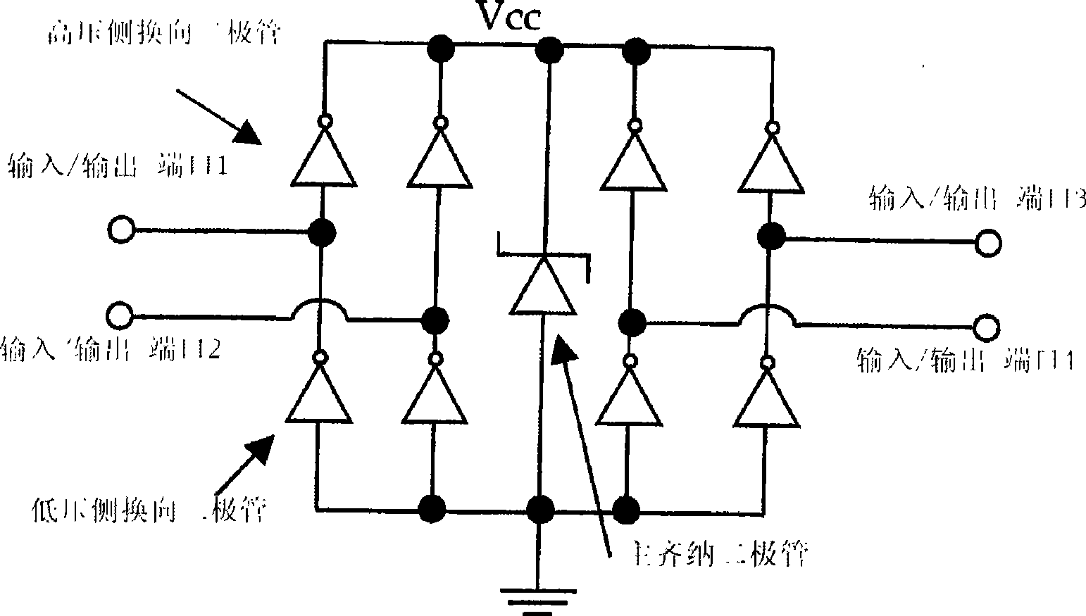
[0022] Figure 3A to Figure 3C is a cross-sectional view showing a TVS clamp diode and high-side / low-side diodes formed on silicon-on-insulator (SOI) of the present invention. A thick body oxide (BOX) layer 110 is deposited on the P-type substrate 105 . The BOX layer 110 has a thickness ranging from 250 Angstroms to 1 micron to withstand an applied breakdown voltage higher than 25V. BOX formation can be achieved by forming a thick oxide layer on the top surface of the P-wafer, then bonding and fusing the oxide layers on the two wafers face-to-face, and finally grinding the substrate to the desired thickness, which is a well-known craft. An optional deep doping implant can be used to convert the P-substrate layer above the BOX layer to a P+ layer. in such as Figure 3A In the illustrated embodiment, the clamping diode is formed in a P-well (PW) 130 on top of an optional P- / P+ substrate layer 120 . The graded doping profile of P-doped region 135 provides trigger voltage reg...


PUM


Abstract

A transient voltage-suppressing (TVS) device supported on a semiconductor substrate is applied to protect an electronic device from a transient voltage. The TVS device includes a clamp diode functions with a high-side and a low side diodes for clamping a transient voltage disposed on a top layer of the semiconductor substrate insulated by a insulation layer constituting a TVS on silicon-on-insulator (SOI) device. In an exemplary embodiment, the insulator layer further includes a thick body oxide (BOX) layer having a thickness in the range of 250 Angstroms to 1 micrometer to sustain an application with a breakdown voltage higher than 25 volts. In another exemplary embodiment, the clamp diode further surrounded by a P-well and the P-well is formed on top of a P- / P+ substrate layer disposed above the insulator layer.

Description

technical field [0001] The present invention generally relates to circuit structures and methods of making transient voltage suppressors (TVS). More specifically, the present invention relates to improved circuit structures and methods for fabricating TVSs in silicon-on-insulator (SOI) layers for providing low capacitance for TVS protection. Background technique [0002] Conventional techniques for designing and manufacturing transient voltage suppressors (TVS) still face certain technical difficulties. In particular, when standard CMOS process steps are applied to form multiple PN junction diodes on a TVS in a semiconductor substrate, inherent PNP and NPN parasitic transistors are created. During an ESD event or when a transient voltage occurs, the parasitic NPN or PNP transistor is turned on or latched as a larger voltage is applied to the TVS array. The latch-up may result in a sudden and strong voltage snap back. Sudden and large jerk returns can have the undesired ef...

Claims


Application Information

Patent Timeline
Patent Type & Authority Applications(China)
IPC IPC(8): H01L27/12H01L23/62H01L21/84
CPCH01L21/84H01L27/1203H01L27/0255H01L29/861H01L29/866H01L29/0649
Inventor 雪克·玛力卡勒强斯瓦密
Owner ALPHA & OMEGA SEMICON INC
Why Eureka
Try Eureka