

Transparent conductive film production method
A technology of transparent conductive film and transparent substrate, which is applied in the direction of electrical digital data processing, input/output process of data processing, ion implantation plating, etc. The effect of over-rate and low sheet resistance
- Summary
- Abstract
- Description
- Claims
- Application Information
AI Technical Summary
Problems solved by technology
Method used
Image

Examples
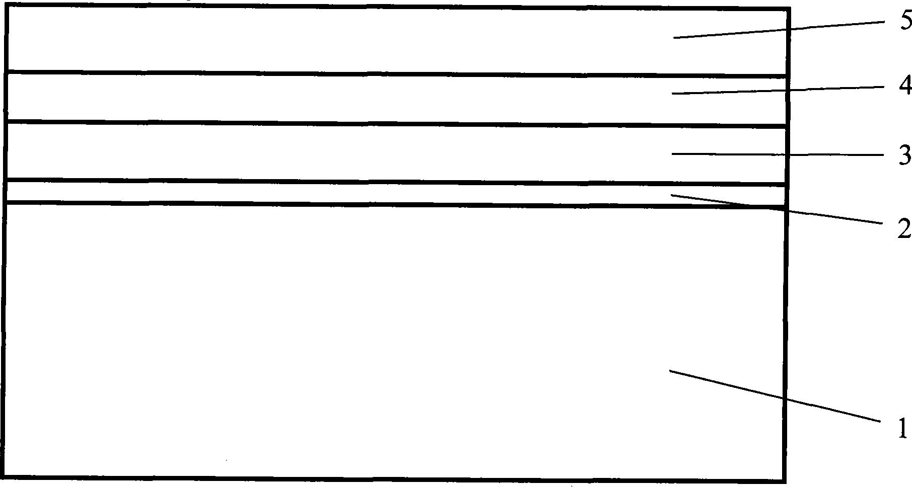
Embodiment 1
[0019] Such as figure 2 As shown, the substrate is a PET film 1 with a thickness of 125 microns and an average transmittance of 91.1% in the visible light range. A buffer layer (silicon dioxide film 2, with a thickness of 4 nm), a low-refractive index transparent conductive film (ITO film 3, with a thickness of 67 nm), and a high-refractive index transparent conductive film (IZO film 4, with a thickness of 4 nm) were sequentially deposited by sputtering. It is 57 nanometers), low refractive index transparent conductive film (ITO film 5, thickness is 70 nanometers). The sheet resistance of the transparent conductive film prepared by the method is 52 ohms, and the average transmittance in the range of visible light is 90.4%.
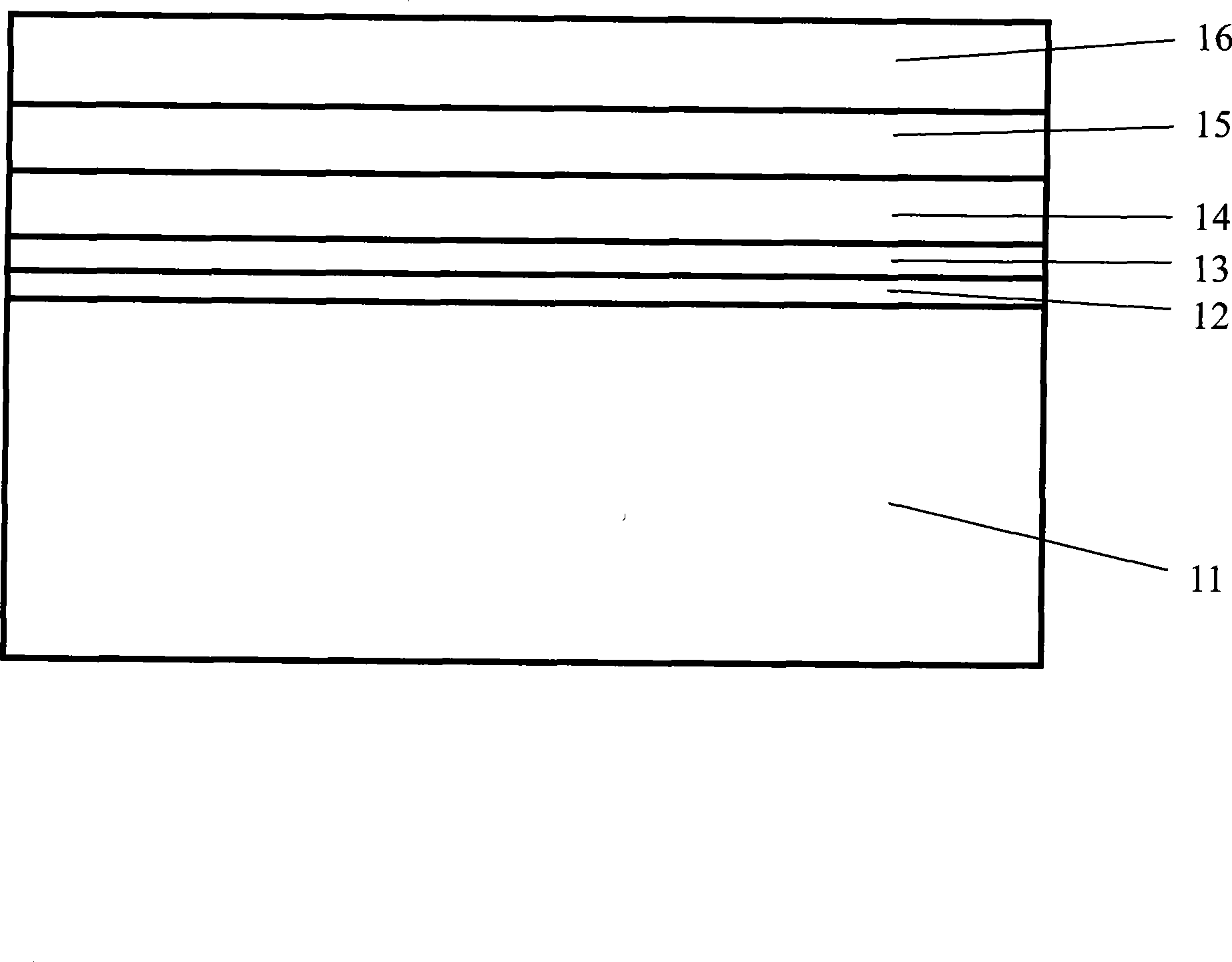
Embodiment 2
[0021] Such as image 3 As shown, the substrate is a PET film 11 with a thickness of 125 microns and an average transmittance of 91.1% in the visible light range. A buffer layer (silicon dioxide film 12, with a thickness of 4 nm), a high-refractive index transparent conductive film (IZO film 13, with a thickness of 5 nm), and a low-refractive index transparent conductive film (ITO film 14, with a thickness of 5 nm) were sequentially deposited by sputtering. 56 nanometers), high refractive index transparent conductive film (IZO film 15, thickness is 57 nanometers), low refractive index transparent conductive film (ITO film 16, thickness is 71 nanometers). The sheet resistance of the transparent conductive film prepared by the method is 53 ohms, and the average transmittance in the range of visible light is 90.5%.
PUM
| Property | Measurement | Unit |
|---|---|---|
| thickness | aaaaa | aaaaa |
| thickness | aaaaa | aaaaa |
| thickness | aaaaa | aaaaa |
Abstract
Description
Claims
Application Information