Supercharge Your Innovation With Domain-Expert AI Agents!

Thermal technique device, method for cleaning translucent element thereof and technique for utilizing the device

A thermal process and component technology, applied in the field of semiconductor process and semiconductor devices, can solve problems such as affecting machine utilization time, increase maintenance cost, product scrap, etc., and achieve the effect of improving process yield, reducing process cost, and reducing replacement frequency.

Inactive Publication Date: 2009-05-20
UNITED MICROELECTRONICS CORP
View PDF0 Cites 0 Cited by
  • Summary
  • Abstract
  • Description
  • Claims
  • Application Information

AI Technical Summary

Problems solved by technology

This approach will not only affect the up-time of the machine, but will also greatly increase the maintenance cost, and there is also the risk of product scrapping

Method used


Image

  • Thermal technique device, method for cleaning translucent element thereof and technique for utilizing the device
  • Thermal technique device, method for cleaning translucent element thereof and technique for utilizing the device

Examples


Embodiment Construction

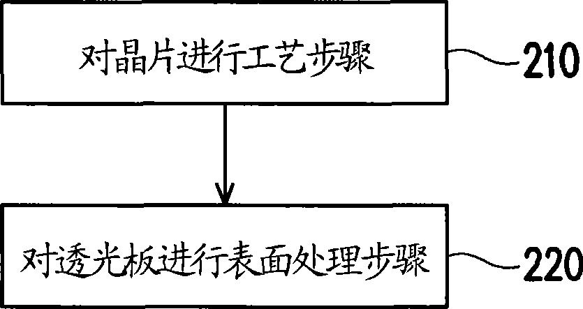
[0039] Hereinafter, examples will be given to further illustrate the present invention, but these examples are not intended to limit the scope of the present invention.

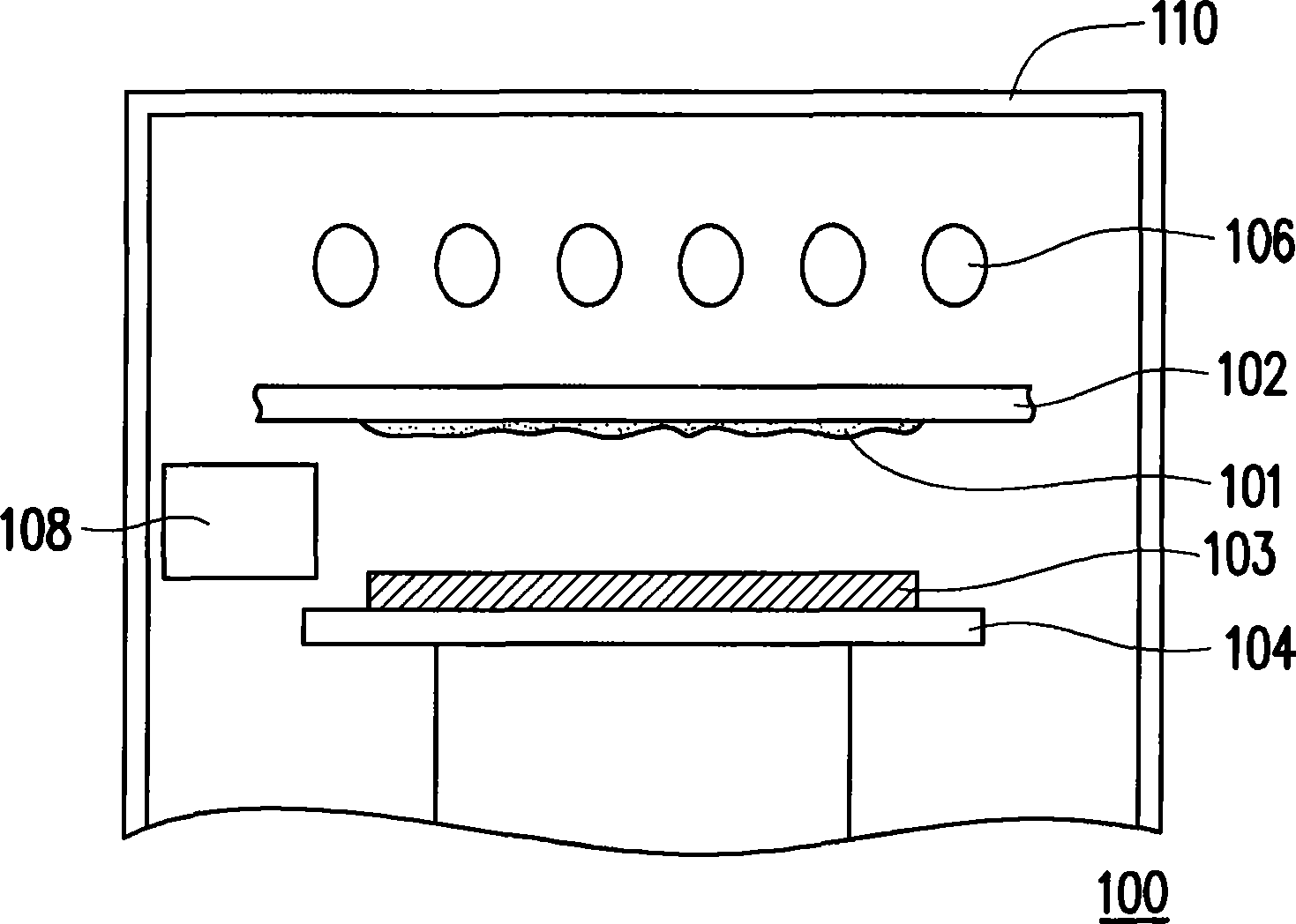
[0040] First, please refer to figure 1, which is a thermal process device according to an embodiment of the present invention. The thermal processing device 100 is suitable for thermal processing in general semiconductor processes, especially for rapid thermal processing (RTP). For example, it is suitable for metal silicide (salicide) process; deposition process for forming silicon oxide, silicon nitride and silicon oxynitride; treatment process for forming low dielectric material; and UV curing process. Of course, it can also be applied to rearrange the crystal lattice and eliminate stress concentration after performing multiple processes such as ion implantation and silicidation, or to form borophospho-silicate glass (Borophospho-silicate Glass, BPSG) and annealing processes such as nitriding.

[0041] T...


PUM


Abstract

The invention discloses a thermal process device, a method for cleaning a light transmission element thereof, and a process using the device. The light transmission element is positioned in a reaction chamber of the device, while the reaction chamber at least comprises a wafer holding seat which is used for bearing a wafer and is arranged below the light transmission element, and also comprises an energy source output element arranged above the light transmission element. The method comprises a surface treating step for cleaning the surface of the light transmission element.

Description

technical field [0001] The invention relates to a semiconductor device and a semiconductor process using the device, and in particular to a method for cleaning a light-transmitting element in a thermal process device, a thermal process and a thermal process device. Background technique [0002] Along with this, the development trend of the semiconductor industry is oriented toward low-cost and high-component-density manufacturing technologies. The Rapid Thermal Processing (RTP) process has gradually replaced the traditional heat treatment step in a high-temperature furnace, and its importance in the future integrated circuit process is beyond doubt. Moreover, this technology has been applied to many semiconductor processes, whether in the field of research or commercial use. [0003] Generally speaking, rapid thermal process (RTP) equipment mainly includes a wafer holder (waferholder) for carrying the wafer; a set of heating lamps (lamp) arranged above the wafer; and a quar...

Claims


Application Information

Patent Timeline
Patent Type & Authority Applications(China)
IPC IPC(8): H01L21/00H01L21/324B08B7/00
Inventor 王裕庸吴兴隆梁昭湖林圣尧施惠绅简佑芳
Owner UNITED MICROELECTRONICS CORP
Features
  • R&D
  • Intellectual Property
  • Life Sciences
  • Materials
  • Tech Scout
  • Unparalleled Data Quality
  • Higher Quality Content
  • 60% Fewer Hallucinations
Learn More