Thin type display device
A technology for thin display devices and substrates, applied in identification devices, AC plasma display panels, instruments, etc., can solve the problems of lack of freedom in the display screen manufacturing process, difficult to bend the screen, heavy large screen, etc., to achieve large screen, Improve process freedom and reduce production cost
- Summary
- Abstract
- Description
- Claims
- Application Information
AI Technical Summary
Problems solved by technology
Method used
Image

Examples
no. 1 approach
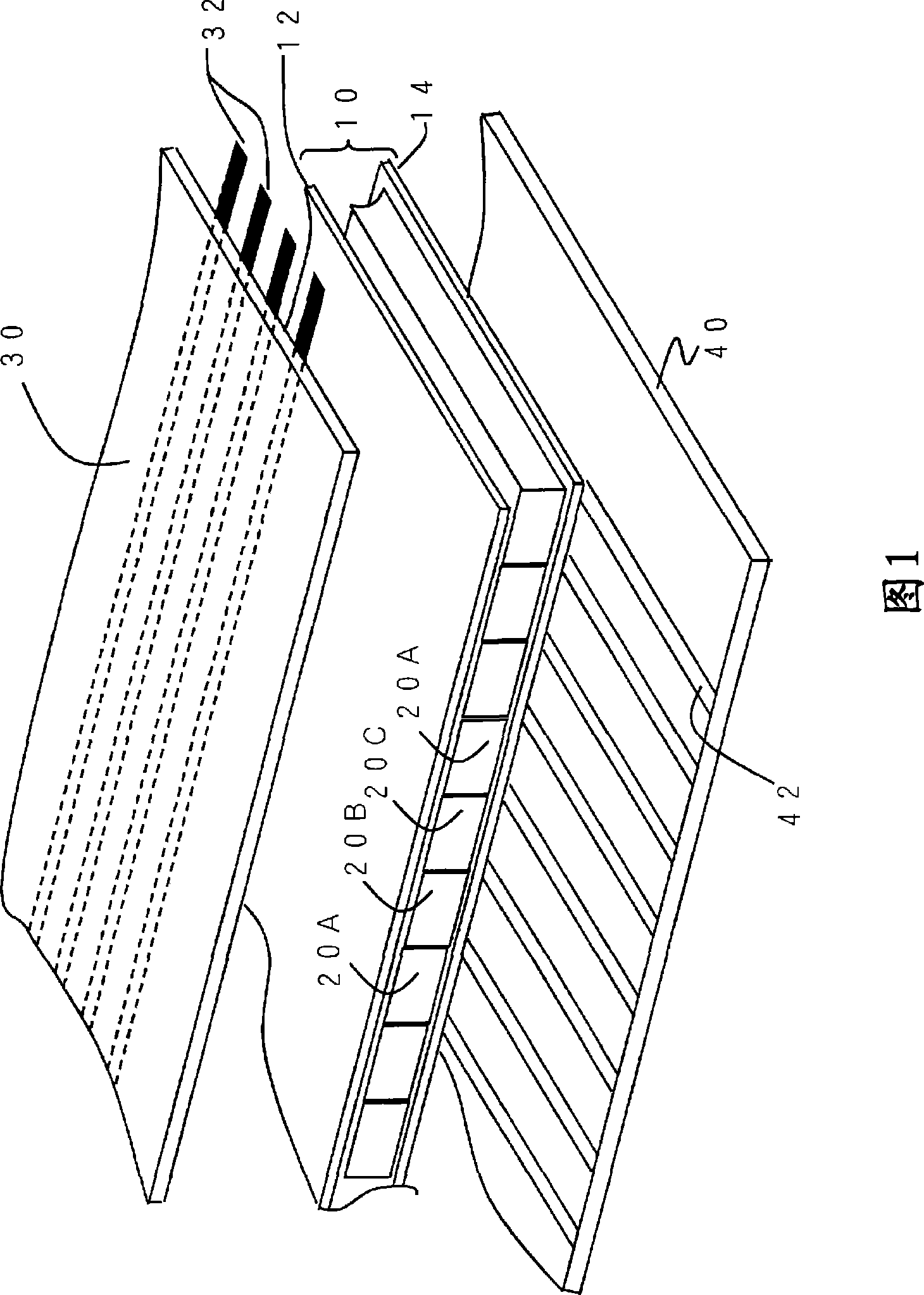
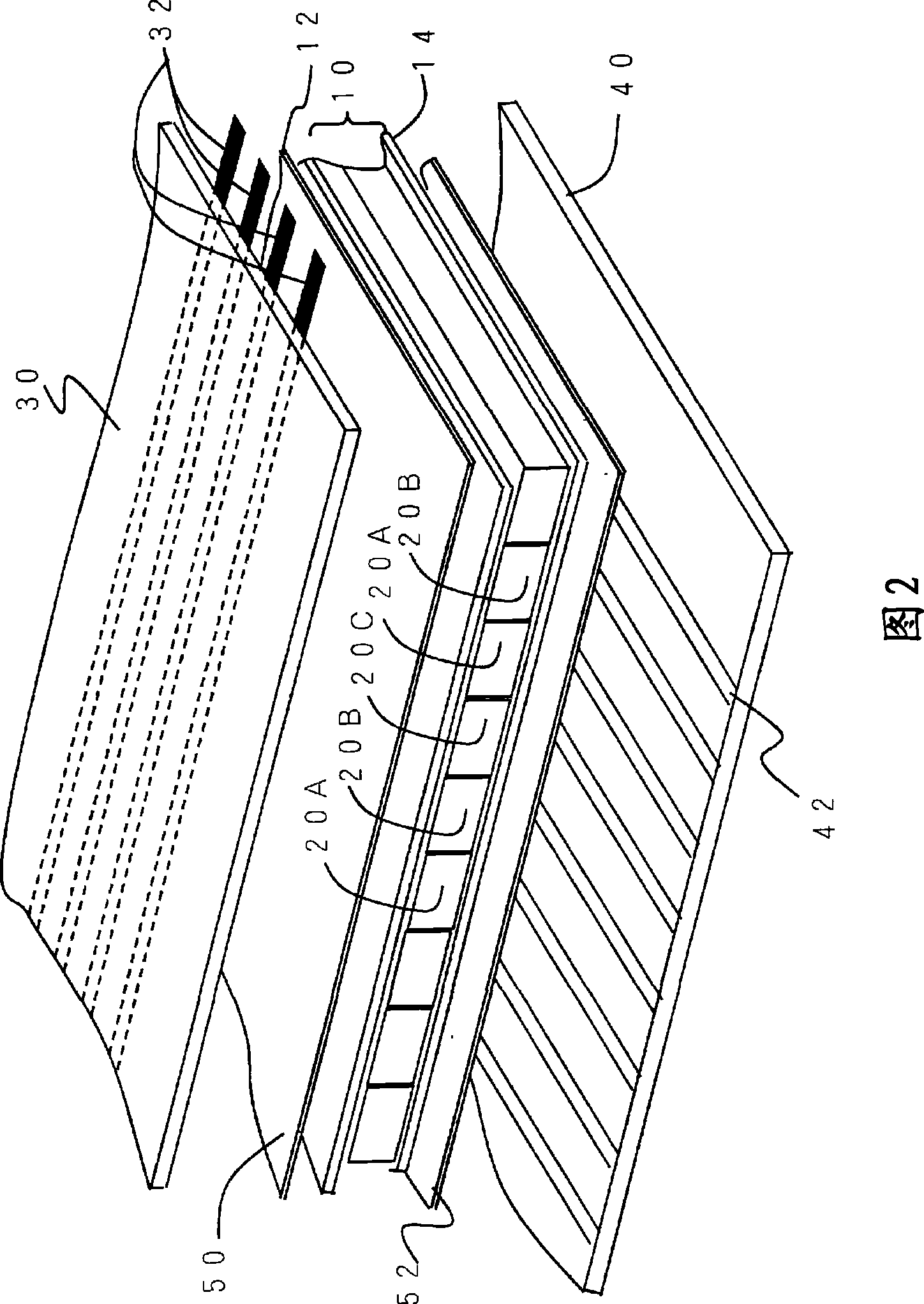
[0036] 1 is a diagram showing the basic structure of the present invention. For example, the light emitting layers 20A, 20B, and 20C of the light emitting part 10 have substrates 12, 14 on the front and back of the light emitting layers that respectively emit red, green, and blue light. The light emitting layers 20A, 20B, and 20C are formed on each substrate by printing. Among the light-emitting layers, for example, the light-emitting layer 20A is a phosphor layer based on ZnS:Sm, Cl, ZnS:Mn, etc., and the light-emitting layer 20B is a phosphor layer based on ZnS:Tb, F, CaS:Ce, etc. , the light emitting layer 20C is a phosphor layer based on ZnS:Tm, F or the like. In addition, the material of the substrates 12 and 14 is an inorganic insulating material, and non-optical materials such as glass or ceramics can be used for the substrate on the rear side. This substrate 12,14 can have the function of insulating layer or dielectric layer, can use BaTiO 3 、 Ta 2 o 5 etc., in the...
no. 2 approach
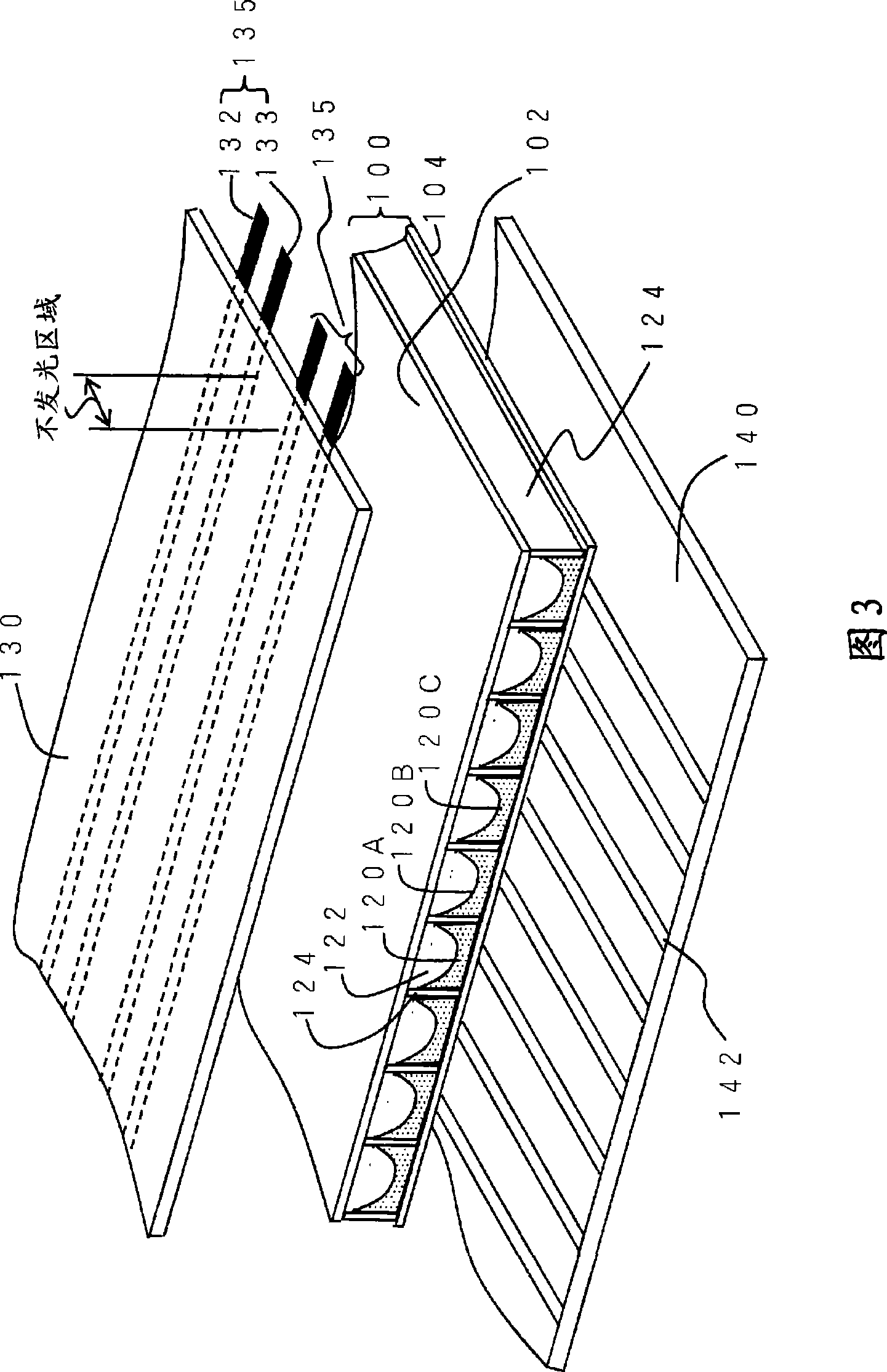
[0042] Next, referring to 3, a display device using gas discharge in the light emitting portion will be described. In FIG. 3 , the light-emitting unit 100 has ribs 124 between the front substrate 102 and the back substrate 104, and discharge gas 122 is enclosed between the ribs 124, and phosphors 120A, 120B, and 120C are sequentially arranged. The bodies emit red, green, and blue light, respectively. The front substrate 102 and the rear substrate 104 are preferably glass substrates of 0.1 mm or less and 30 μm or more, similar to the substrates 12 and 14 in FIGS. 1 to 2 . In addition, the front substrate 102 is preferably a translucent glass substrate, while the rear substrate 104 may not have translucency, or may be a glass substrate containing a pigment. Also, although not shown, a protective film such as a HgO film is formed on the contact surfaces of front substrate 102 and ribs 124 with discharge gas 122 to prevent damage from plasma generated during discharge.
[0043] ...
no. 3 approach
[0057] FIG. 4 shows a configuration of a display device 200 that uses a combination of the thin display device shown in FIG. 3 and peripheral circuits.
[0058] A driving mechanism 500 is connected to the display device 200. In this embodiment, the sustain electrode pairs 135 extend in the row direction of the display screen, and each sustain electrode pair 135 has a paired structure of a scan / sustain Y electrode and a sustain X electrode. The region where the sustain electrode pair 135 intersects the address electrode 142 is called a cell, and when selecting a cell that emits light in accordance with the discharge between the sustain electrode pair 135 in each cell, the scan / hold Y electrode is used as a scan electrode that selects the cell in a row unit. . The address electrodes 142 extend in the column direction and serve as electrodes for selecting cells in units of columns. The drive mechanism 500 has a controller 512, a data processing circuit 514, an X driver 516, a sc...
PUM
 Abstract
Description
Claims
Application Information
 - R&D
- Intellectual Property
- Life Sciences
- Materials
- Tech Scout
- Unparalleled Data Quality
- Higher Quality Content
- 60% Fewer Hallucinations
Browse by: Latest US Patents, China's latest patents, Technical Efficacy Thesaurus, Application Domain, Technology Topic, Popular Technical Reports.
© 2025 PatSnap. All rights reserved.Legal|Privacy policy|Modern Slavery Act Transparency Statement|Sitemap|About US| Contact US: help@patsnap.com