Electrophoretic display device, method for driving electrophoretic display device, and electronic apparatus

An electrophoretic display and electrophoresis technology, applied in static indicators, nonlinear optics, instruments, etc., can solve the problems of increased power consumption, high-precision correspondence difficulties, and panel current consumption cannot be ignored, etc., to achieve power saving, The effect of suppressing manufacturing variation

Inactive Publication Date: 2009-05-27
SEIKO EPSON CORP
View PDF1 Cites 5 Cited by
  • Summary
  • Abstract
  • Description
  • Claims
  • Application Information

AI Technical Summary

Problems solved by technology

In this way, since the average area per pixel increases, it becomes difficult to respond to high-definition. Furthermore, because the through current at the time of writing the image signal (when charging the capacitance of the driving

Method used


Image

  • Electrophoretic display device, method for driving electrophoretic display device, and electronic apparatus
  • Electrophoretic display device, method for driving electrophoretic display device, and electronic apparatus
  • Electrophoretic display device, method for driving electrophoretic display device, and electronic apparatus

Examples


no. 1 Embodiment approach

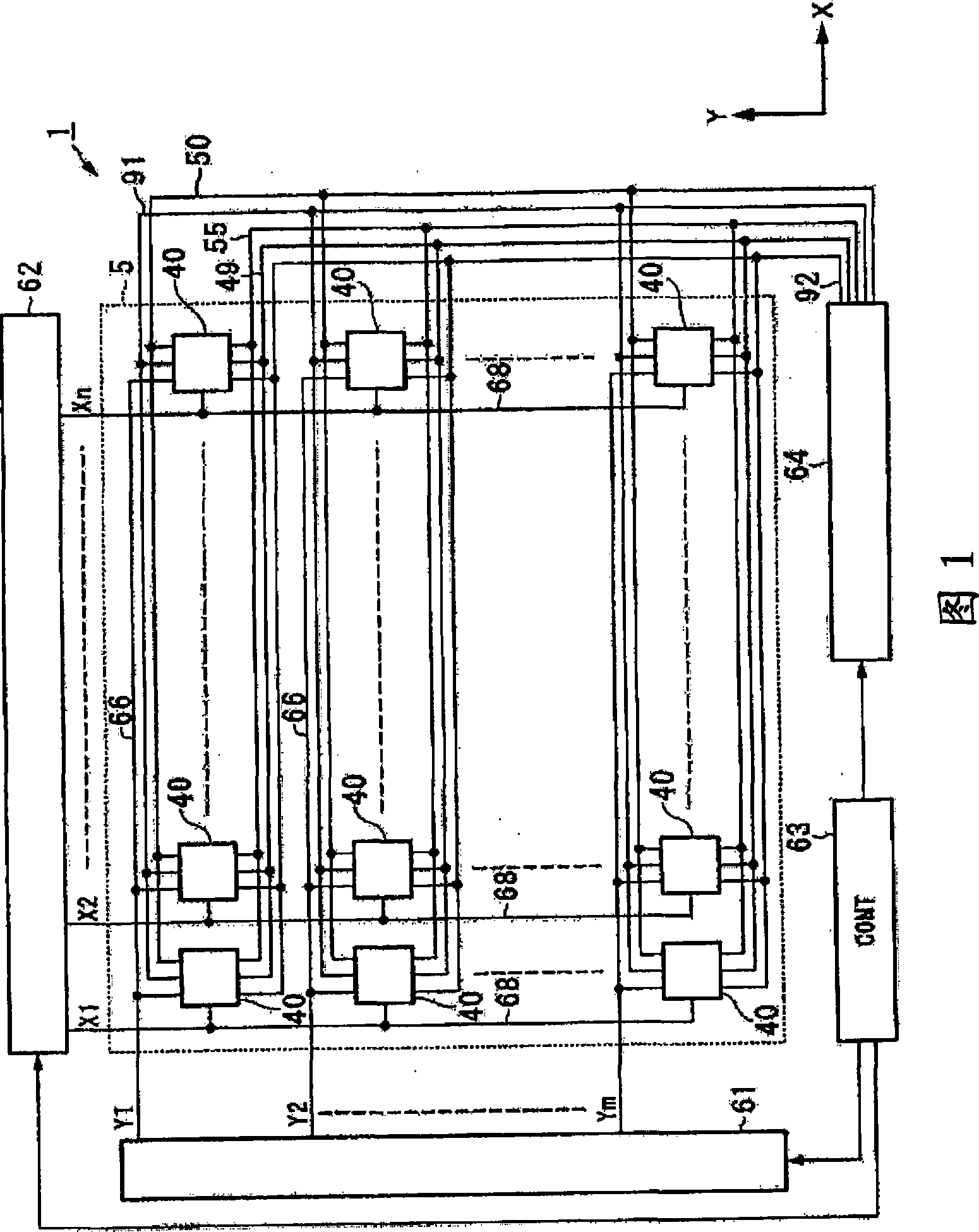
[0064] FIG. 1 is a schematic configuration diagram of an electrophoretic display device 1 of an active matrix driving method.

[0065] The electrophoretic display device 1 includes a display unit 5 in which a plurality of pixels 40 are arranged. Around the display unit 5, a scanning line driving circuit 61, a data line driving circuit 62, a controller (control unit) 63, and a common power modulation circuit 64 are arranged. The scanning line driving circuit 61 , the data line driving circuit 62 , and the common power modulation circuit 64 are respectively connected to the controller 63 . The controller 63 comprehensively controls them based on image data, synchronization signals, and the like supplied from a higher-level device.

[0066] A plurality of scanning lines 66 extending from the scanning line driving circuit 61 and a plurality of data lines 68 extending from the data line driving circuit 62 are provided in the display unit 5 , and pixels 40 are provided correspondin...

no. 2 Embodiment approach

[0157] Next, a second embodiment of the present invention will be described.

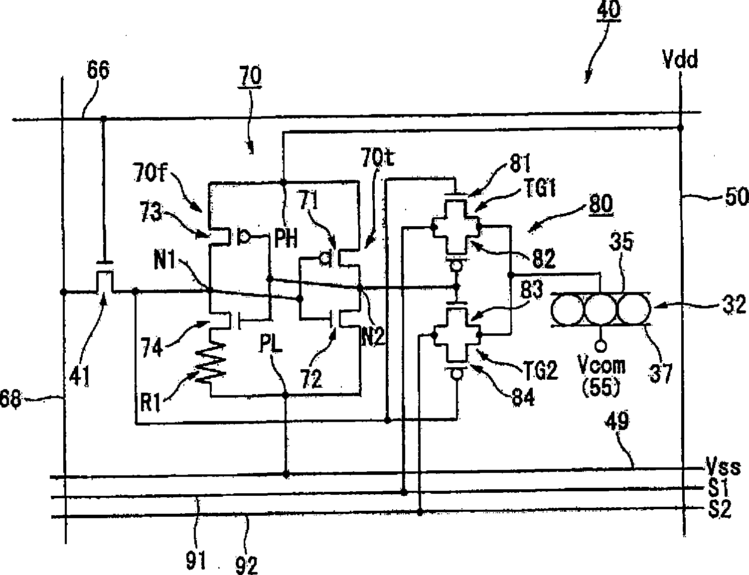
[0158] FIG. 10 is a circuit configuration diagram of a pixel 240 included in the electrophoretic display device in the second embodiment. Also, in Figure 10, with figure 2 The same symbols are attached to the same constituent elements, and their detailed descriptions are appropriately omitted.

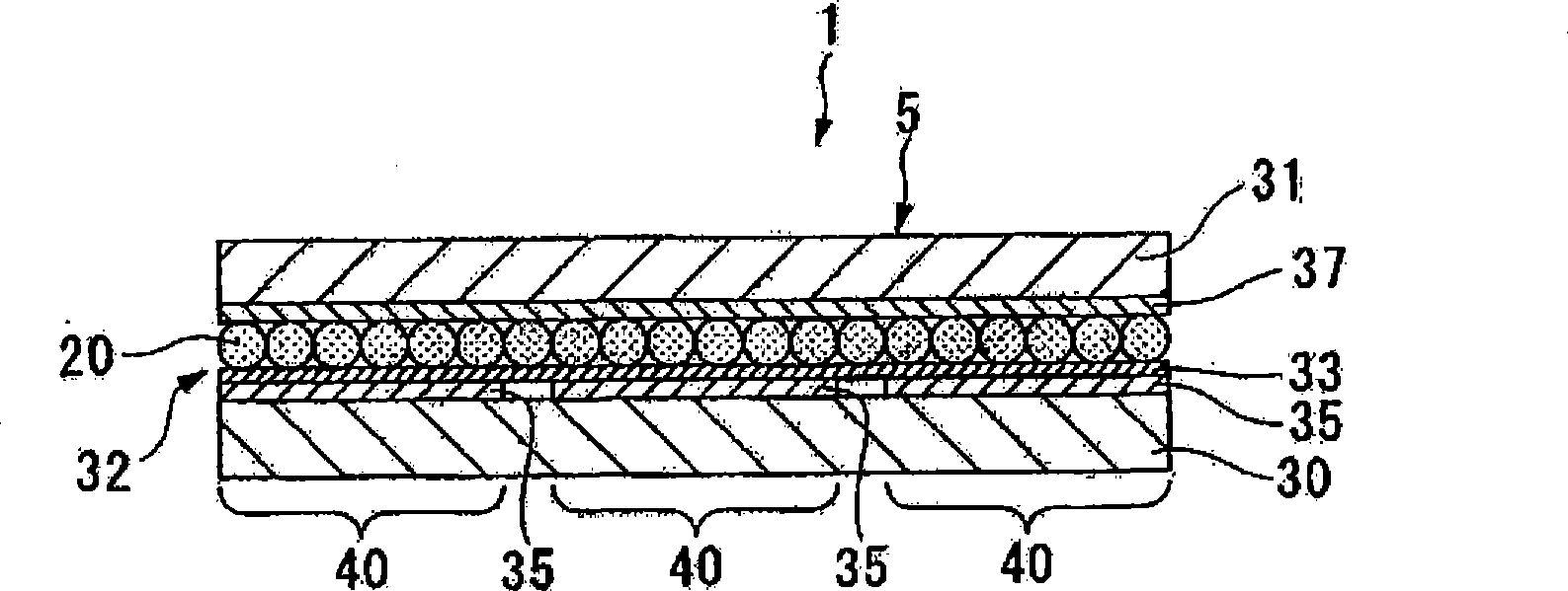
[0159] A pixel 240 shown in FIG. 10 includes a driving TFT 41 , a latch circuit (storage circuit) 270 , a switch circuit 80 , a pixel electrode 35 , an electrophoretic element 32 , and a common electrode 37 . In addition, because the configuration other than the latch circuit 270 (the driving TFT 41, the switch circuit 80, etc.) is the same as that shown in figure 2 The pixel 40 is the same, so the latch circuit 270 will be mainly described below.

[0160] The latch circuit 270 includes a transfer inverter 270 t , a feedback inverter 270 f , and a switching transistor 75 .

[0161] transfer inverter 27...


PUM


Abstract

The present invention relates to an electrophoretic display device, driving method and electronic apparatuses thereof. The electrophoretic display device has excellent manufacturability, operational reliability and electricity-saving property, and may prevent generation of fault operation of memory circuit caused by element deviation. The electrophoretic display device includes, on each pixel, a TFT (41) for setting drive, a latch circuit connecting between the TFT (41) for drive and pixel electrodes (35); the latch circuit (70) comprises: a transfer inverter (70t), which has an input terminal for connecting the TFT (41) for drive and an output terminal for connecting the pixel electrodes (35); a feedback inverter (70f), which has an input terminal connecting with the output terminal of the transfer inverter (70t), and an output terminal connecting with the TFT (41) for drive; and a resistance element (R1) connecting with low-potential source side of the feedback inverter (70f), and having resistance value larger than conductive resistance and less than crossover resistance of a N-MOS transistor (74) of the feedback inverter (70f).

Description

technical field [0001] The present invention relates to an electrophoretic display device, a driving method of the electrophoretic display device, and electronic equipment. Background technique [0002] As an active matrix type electrophoretic display device, an electrophoretic display device including a switching transistor and a memory circuit in a pixel is known (for example, refer to Patent Document 1). In the display device described in Patent Document 1, microcapsules containing charged particles are attached to a first substrate on which pixel switching transistors and pixel electrodes are formed. In addition, the microcapsules are sandwiched between the counter electrode formed on the second substrate side and the pixel electrode on the first substrate side, and the charged particles are controlled by the electric field generated between the pixel electrode and the counter electrode to perform image processing. show. [0003] [Patent Document 1] JP-A-2003-84314 Gaz...

Claims


Application Information

Patent Timeline
IPC IPC(8): G02F1/167G09G3/34
CPCG09G2300/0857
Inventor 下平泰裕
Owner SEIKO EPSON CORP
Why Eureka
Try Eureka