
Method for manufacturing nano-scale pattern

A nano-scale, graphic technology, used in the manufacture of microstructure devices, photoengraving processes for patterned surfaces, processes for producing decorative surface effects, etc. Solve high-cost, high-resolution, low-cost effects

Active Publication Date: 2009-05-27
新疆中科丝路物联科技有限公司
View PDF0 Cites 3 Cited by
  • Summary
  • Abstract
  • Description
  • Claims
  • Application Information

AI Technical Summary

Problems solved by technology

[0005] In view of this, the main purpose of the present invention is to provide a method for producing nanoscale patterns using electron beams produced by field emission, to effectively solve the problems of high cost of immersion lithography and proximity effect of focused electron beams affecting resolution

Method used

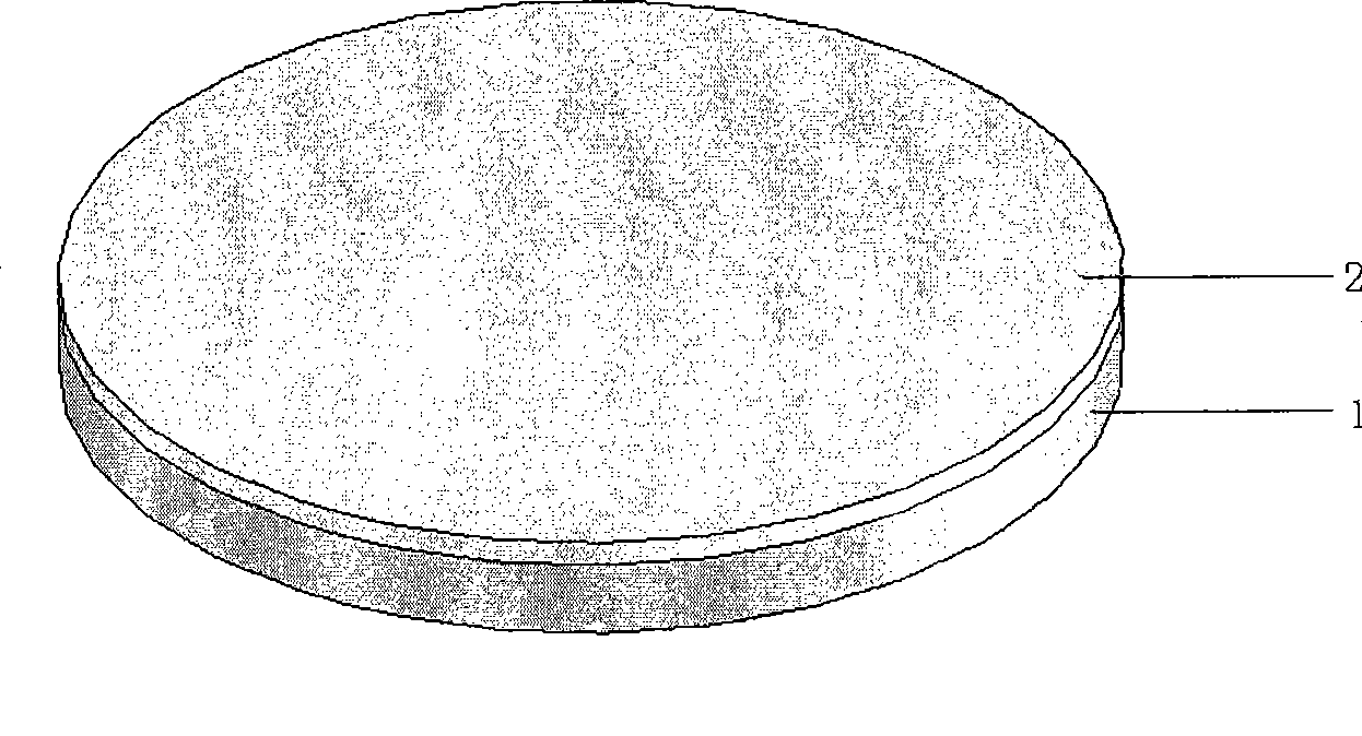
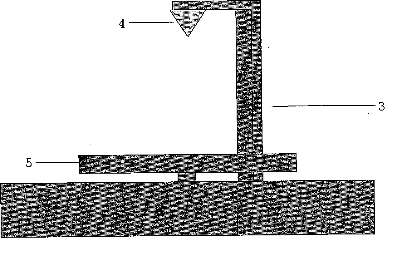

Image

  • Method for manufacturing nano-scale pattern
  • Method for manufacturing nano-scale pattern
  • Method for manufacturing nano-scale pattern

Examples


Embodiment Construction

[0027] In order to make the object, technical solution and advantages of the present invention clearer, the present invention will be described in further detail below in conjunction with specific embodiments and with reference to the accompanying drawings.

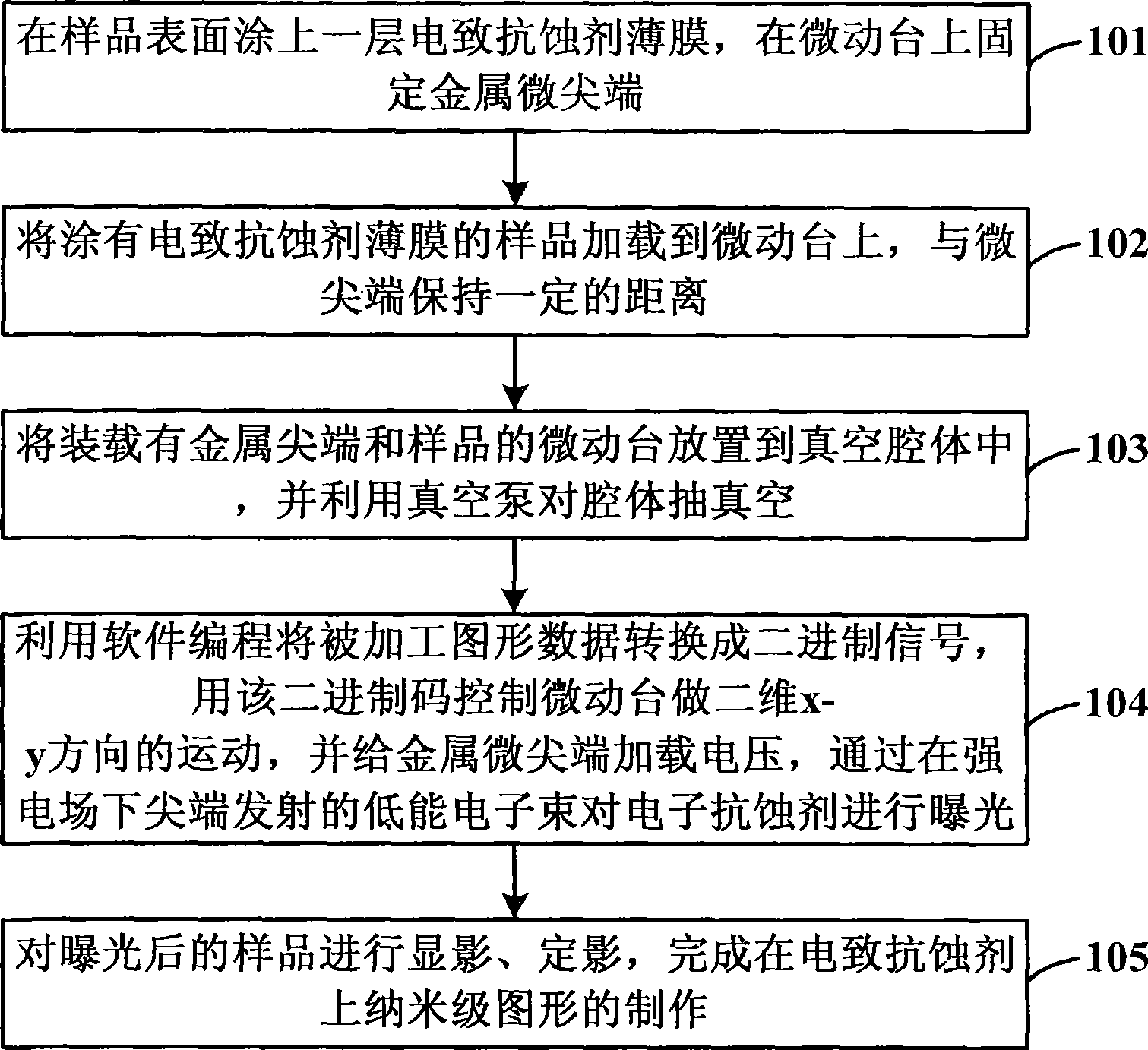
[0028] Such as figure 1 as shown, figure 1 It is a flow chart of the method for making nanoscale graphics using electron beams generated by field emission provided by the present invention. The nanoscale graphics convert graphic data into binary signals to control the two-dimensional x-y direction movement of the micro-motion stage and the loading of the metal tip voltage , obtained by exposing the electronic resist with an electron beam generated after the tip is loaded with a voltage, the method includes:

[0029] Step 101: Coating a layer of electroresist film on the surface of the sample, and fixing the metal microtip on the micro-motion stage; in this step, a layer of electroresist is coated on the surface of the sa...


PUM


Abstract

The invention discloses a method for preparing a nanometer pattern. Pattern data is converted into a binary signal to control the movement of a microchecker in the two-dimensional x-y direction and the loading of the metal tip voltage; and the nanometer pattern is obtained through the exposure of an electronic resist by the electron beam produced by the loaded tip voltage. The method comprises the following steps: coating an electric resist film onto the surface of a sample, and fixing a metal micro-tip on the microchecker; loading the sample coated with the electric resist film onto the microchecker, and keeping a certain distance from the micro-tip; placing the microchecker loaded with the metal tip and the sample into a vacuum cavity, and vacuumizing the cavity through a vacuum pump; converting the pattern data to be processed into the binary signal through software programming, using the binary code to control the microchecker to move in the two-dimensional x-y direction, loading the voltage to the metal micro-tip, and exposing the electronic resist through the low-energy electron beam emitted by the tip in a strong electric field; and carrying out the development and fixation of the exposed sample. The method effectively solves the problems that the immersed type photolithography has high cost; and a focused electron beam has a proximity effect on the resolution.

Description

technical field [0001] The invention relates to the technical field of deep submicron and nanometer processing in microelectronic technology, in particular to a method for making nanometer-scale graphics by using electron beams generated by field emission. Background technique [0002] With the rapid development of the semiconductor industry, the feature size of the device has comprehensively entered the nanometer scale from deep submicron. The ability of nanoscale pattern processing has become the key to determine that integrated circuits continue to advance downwards according to Moore's law. At the same time, with the vigorous rise of nanoscience, nanoscale pattern processing has become the basis for the development of nanotechnology. [0003] At present, immersion lithography technology and focused electron beam lithography are generally used to realize nanoscale pattern processing. However, the above-mentioned immersion lithography technology has the problem of high i...

Claims


Application Information

Patent Timeline
IPC IPC(8): G03F7/00B81C1/00
Inventor 傅剑宇陈大鹏景玉鹏欧毅叶甜春
Owner 新疆中科丝路物联科技有限公司
Learn More