Multilayer tablet fuse and method of manufacturing the same

A multi-layer chip, fuse technology, applied in fuse manufacturing, emergency protection devices, electrical components, etc., can solve the problems of not being widely used, large equipment investment, long production cycle, etc., to achieve shortened production cycle, equipment The effect of low investment and simple process

Active Publication Date: 2009-05-27
NANJING SART SCI & TECH DEV
View PDF0 Cites 12 Cited by
  • Summary
  • Abstract
  • Description
  • Claims
  • Application Information

AI Technical Summary

Problems solved by technology

[0003] The fuse of the above-mentioned multi-layer fuse adopts a monolithic process, which is complicated,

Method used


Image

  • Multilayer tablet fuse and method of manufacturing the same
  • Multilayer tablet fuse and method of manufacturing the same
  • Multilayer tablet fuse and method of manufacturing the same

Examples


Example Embodiment

[0029] Example 1: Preparation of three-layer chip fuse

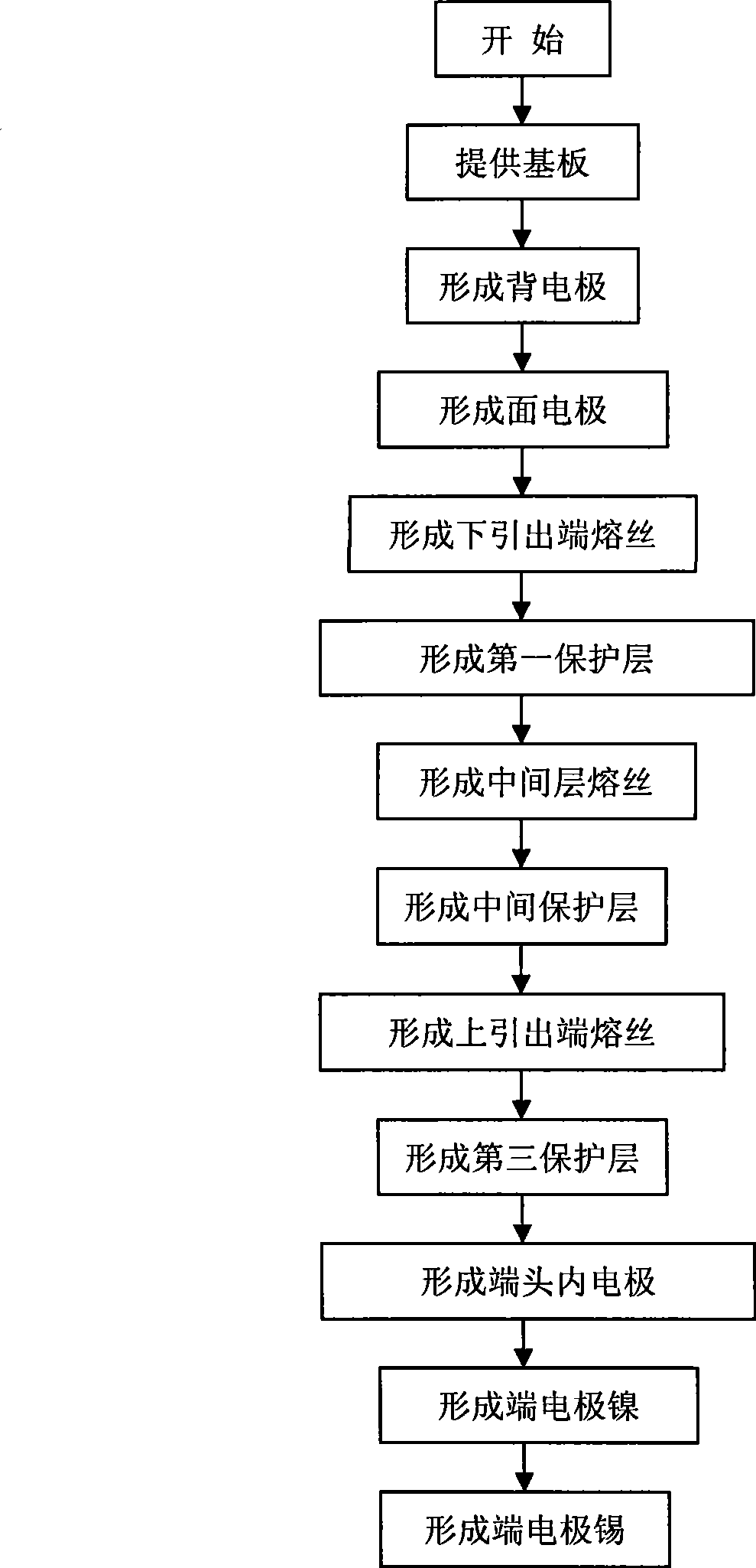
[0030] The preparation process is as figure 1 As shown, the specific operations are as follows:

[0031] One: Provide substrate 1, mainly made of alumina or steatite porcelain, such as figure 2 ;

[0032] 2: Form the back electrode

[0033] Such as image 3 As shown, on the left and right sides of the lower surface of the substrate 1, the back electrode pattern 2 is formed by screen printing conductive paste, and the conductive paste material contains silver;

[0034] 3. Put it in a drying oven to dry (temperature: 150℃, time: 15min)

[0035] 4: Form the front electrode

[0036] Such as Figure 4 As shown, the front electrode 3 is formed by screen printing conductive paste on the front surface of the substrate 1, and the material contains silver or silver palladium;

[0037] 5. Put it in a drying oven to dry (temperature: 150℃, time: 15min)

[0038] 6. Put into sintering furnace for sintering (maximum temperature: 600℃ - 8...

Example Embodiment

[0063] Example 2:

[0064] The S1206-S-0.5A product is made through the above example 1, and tested in accordance with the inspection items and technical requirements of GB9364.4-2006 and GB9364.1-1997, which fully meets the performance requirements, especially the 10 times current anti-surge test Compared with the traditional single-layer chip fuse, the result is greatly improved. For the convenience of explanation, the comparison table of the above test is listed:

[0065] Table 1: Comparison of aging test

[0066]

[0067] Note: The test conditions are: 20 samples are taken from each, the rated current is applied for 200h at a temperature of 25°C and a humidity of 40%, and the fusing time of twice the current and ten times the current after the end of the sample.

[0068] Instruments used in this experiment: BXC-35A fuse tester, DS5062M digital oscilloscope.


PUM


Abstract

The invention belongs to the field of fuse plug, and in particular relates to a multilayer SMD fuse and a preparation method thereof. The multi-layer SMD fuse consists of a ceramic substrate, a back electrode, face electrodes, fuse wires, protective layers and a metal end head, wherein the fuse wires are multilayer, fuse wires of adjacent layers are connected end to end, two end heads of connected fuse wires are connected with the face electrodes on two sides of the substrate respectively, and each layer of fuse wire is provided with a protective layer. When the fuse is prepared, except the uppermost protective layer, each protective layer does not cover the tail end of the fuse wire, so that the multilayer fuse wires are connected end to end to form a cascaded structure. Compared with the prior art, the invention has the advantages of simpler procedure, smaller equipment input, shorter production period and lower cost.

Description

technical field [0001] The invention belongs to the field of fuses, and in particular relates to a chip fuse for protecting electronic components and a preparation method thereof. Background technique [0002] Most of the existing fuses use the production process of chip resistors, which can only print a layer of fuse. Although the shape of the fuse can be various, such as linear, Great Wall, snake, etc., its length will still vary. It is very limited and cannot meet the needs of high surge resistance in many occasions. There is another kind of fuse, which can print multi-layer fuses, which can meet the anti-surge requirements in many occasions. It is composed of three or more layers of glass ceramic material layers and a metal film deposited on each layer to form a monolithic structure. , the two ends of this monolithic structure are covered with a conductive layer, and the inside is connected by a metal film arranged in parallel. It is covered with a layer of metal film o...

Claims


Application Information

Patent Timeline
IPC IPC(8): H01H85/046H01H69/02
Inventor 陆秀荣南式荣杨漫雪
Owner NANJING SART SCI & TECH DEV
Why Eureka
Try Eureka