Device structure of SONOS memory tube and method for producing the same

A device structure and storage tube technology, which is applied to the device structure of SONOS storage tube and the field of fabrication of the device structure, can solve the problems of limited use and promotion of SONOS devices, large storage unit area, etc. area reduction effect

Inactive Publication Date: 2009-05-27
SHANGHAI HUA HONG NEC ELECTRONICS
View PDF0 Cites 16 Cited by
  • Summary
  • Abstract
  • Description
  • Claims
  • Application Information

AI Technical Summary

Problems solved by technology

However, the area of ​​the storage unit of the usual SONOS structure is relatively large, which limits the use and promotion of SONOS devices.

Method used


Image

  • Device structure of SONOS memory tube and method for producing the same
  • Device structure of SONOS memory tube and method for producing the same
  • Device structure of SONOS memory tube and method for producing the same

Examples


Embodiment Construction

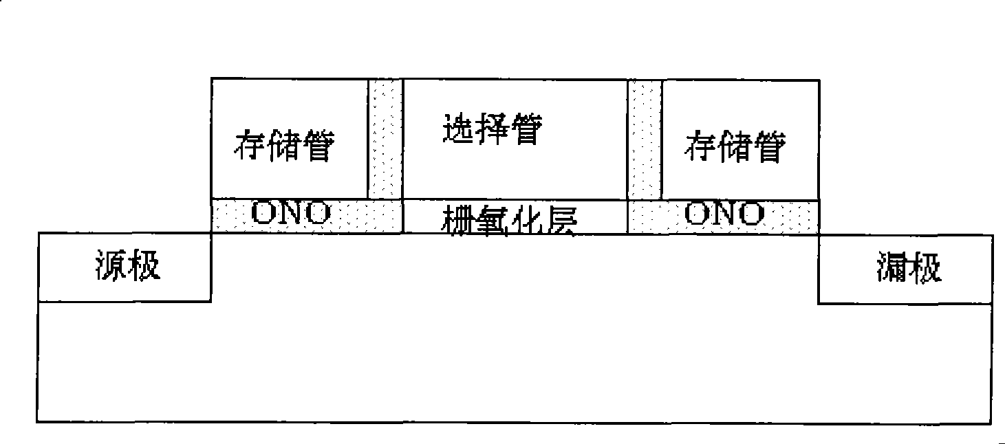
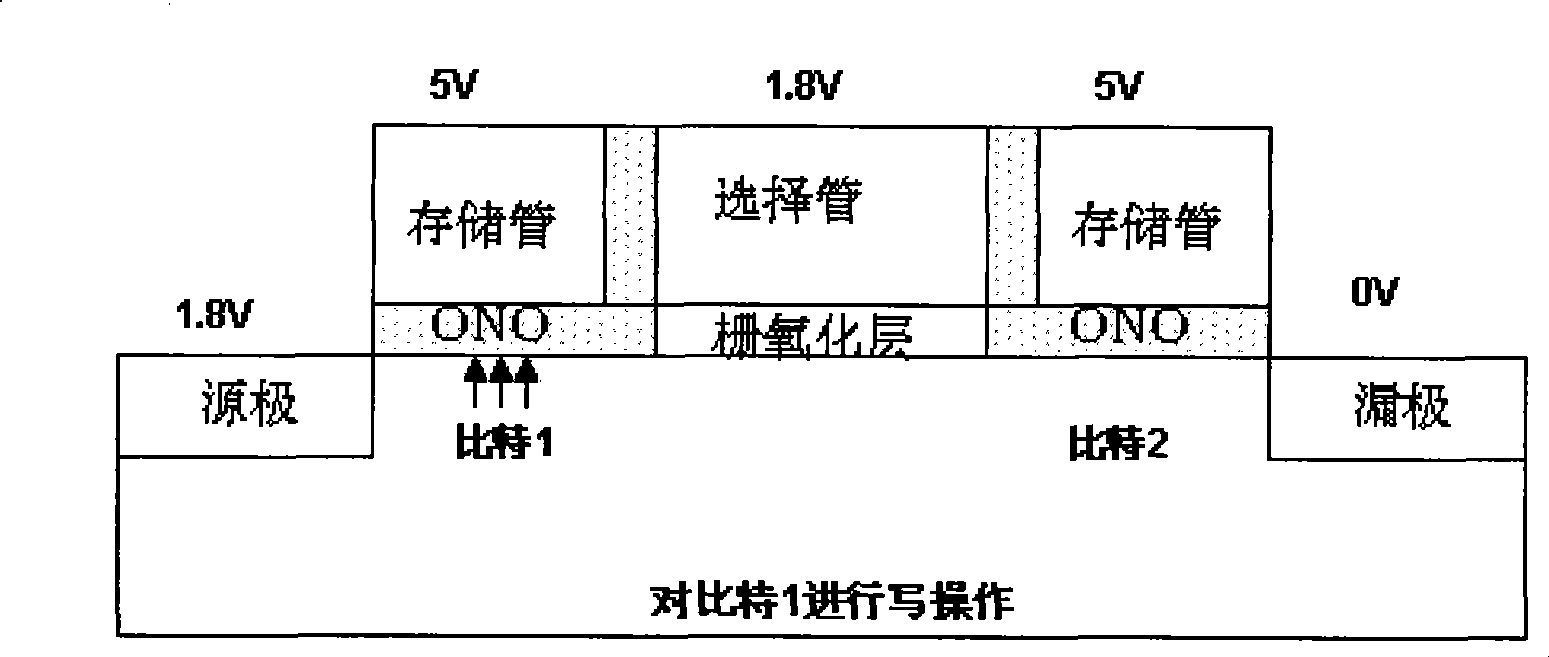
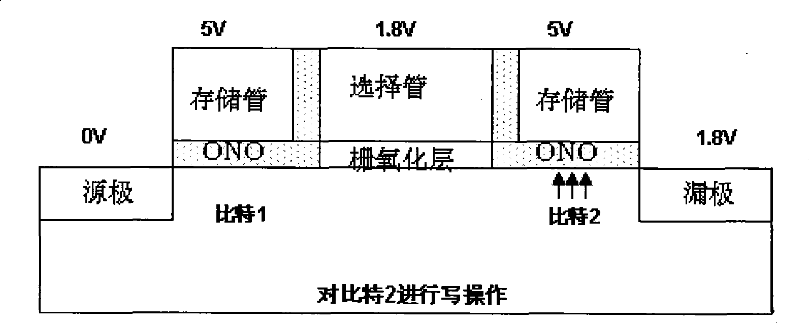
[0021] The invention provides a device structure of a SONOS storage tube, such as figure 1 As shown, a gate oxide layer is arranged on the middle of the substrate, a selection transistor is arranged above the gate oxide layer, and an "L"-shaped ONO layer with a gap facing outward is respectively arranged on both sides of the gate oxide layer and the selection transistor. The gap position of the ONO layer is provided with a storage tube, and on the substrate outside the two storage tubes and the ONO layer, a source is provided on one side and a drain is provided on the other side.

[0022] The ONO layer includes two silicon dioxide layers and a silicon nitride layer sandwiched between the two silicon dioxide layers, and the thickness of the lower silicon dioxide layer is 15 to 25 , the thickness of the middle silicon nitride layer is 60-120 , the thickness of the upper silicon dioxide layer is 40 to 80 .

[0023] In the device structure of the SONOS memory tube of the pre...


PUM


Abstract

The invention discloses a device structure of an SONOS storage tube. The middle part of a substrate is provided with a gate oxide layer, and a selection tube is arranged above the gate oxide layer; both sides of the gate oxide layer and the selection tube are provided with L-shaped ONO layers with outward gap respectively; the storage tubes are arranged on the gaps of the ONO layers; and on the substrate of the two storage tubes and the outer side of the ONO layers, one side is provided with a source electrode, while the other side is provided with a drain electrode. The invention also discloses a method for manufacturing the device structure of the SONOS storage tube, wherein the side wall is etched to form the SONOS storage tube, and a dibit SONOS storage unit simultaneously; and the manufacturing method is simple in procedure and easy to implement; moreover, the area of the storage unit occupied by the SONOS storage tube is greatly reduced, and the performance of the device is improved.

Description

technical field [0001] The invention relates to a semiconductor device, in particular to a device structure of a SONOS storage tube. The invention also relates to a manufacturing method of the device structure of the SONOS storage tube. Background technique [0002] The charge trapping device is a structure with very good electrical performance for shrinking the flash memory, and this structure is the trend of technical development in this field. Moreover, this device has a very simple manufacturing process, which is very convenient for mass production. This device is the so-called SONOS device (polysilicon-oxide-nitride-oxide-silicon, polysilicon-silicon dioxide-silicon nitride- silica - silicon). However, the area of ​​the storage unit of the usual SONOS structure is relatively large, which limits the use and promotion of SONOS devices. Contents of the invention [0003] The technical problem to be solved by the present invention is to provide a device structure of a ...

Claims


Application Information

Patent Timeline
Patent Type & Authority Applications(China)
IPC IPC(8): H01L29/792H01L29/423H01L27/115H01L21/336H01L21/28H01L21/8247
Inventor 孙亚亚
Owner SHANGHAI HUA HONG NEC ELECTRONICS
Why Eureka
Try Eureka