Semiconductor device with surge current protection and method of making the same

A manufacturing method and semiconductor technology, applied in the direction of semiconductor devices, electrical components, circuits, etc., can solve problems such as inapplicability

Inactive Publication Date: 2009-06-03
PI
View PDF10 Cites 5 Cited by
  • Summary
  • Abstract
  • Description
  • Claims
  • Application Information

AI Technical Summary

Problems solved by technology

However, the mesa edge termination technology for Si cannot generally be applied to SiC device technology because of the difficult

Method used


Image

  • Semiconductor device with surge current protection and method of making the same
  • Semiconductor device with surge current protection and method of making the same
  • Semiconductor device with surge current protection and method of making the same

Examples


Embodiment Construction

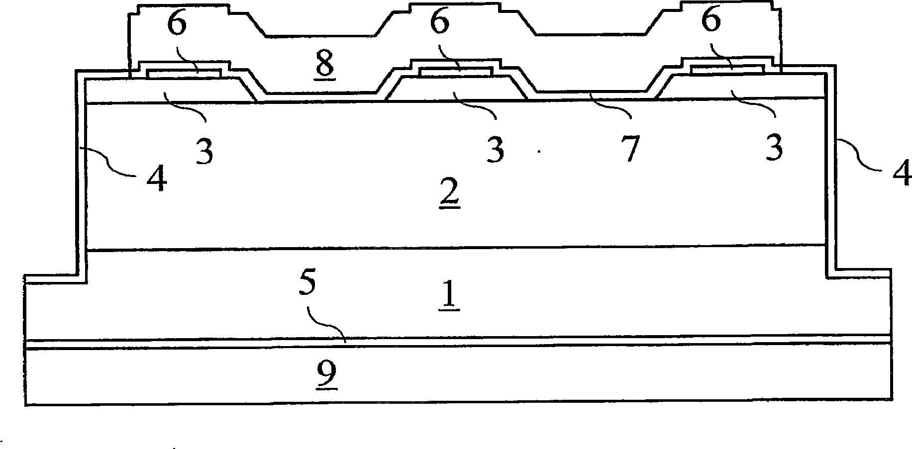
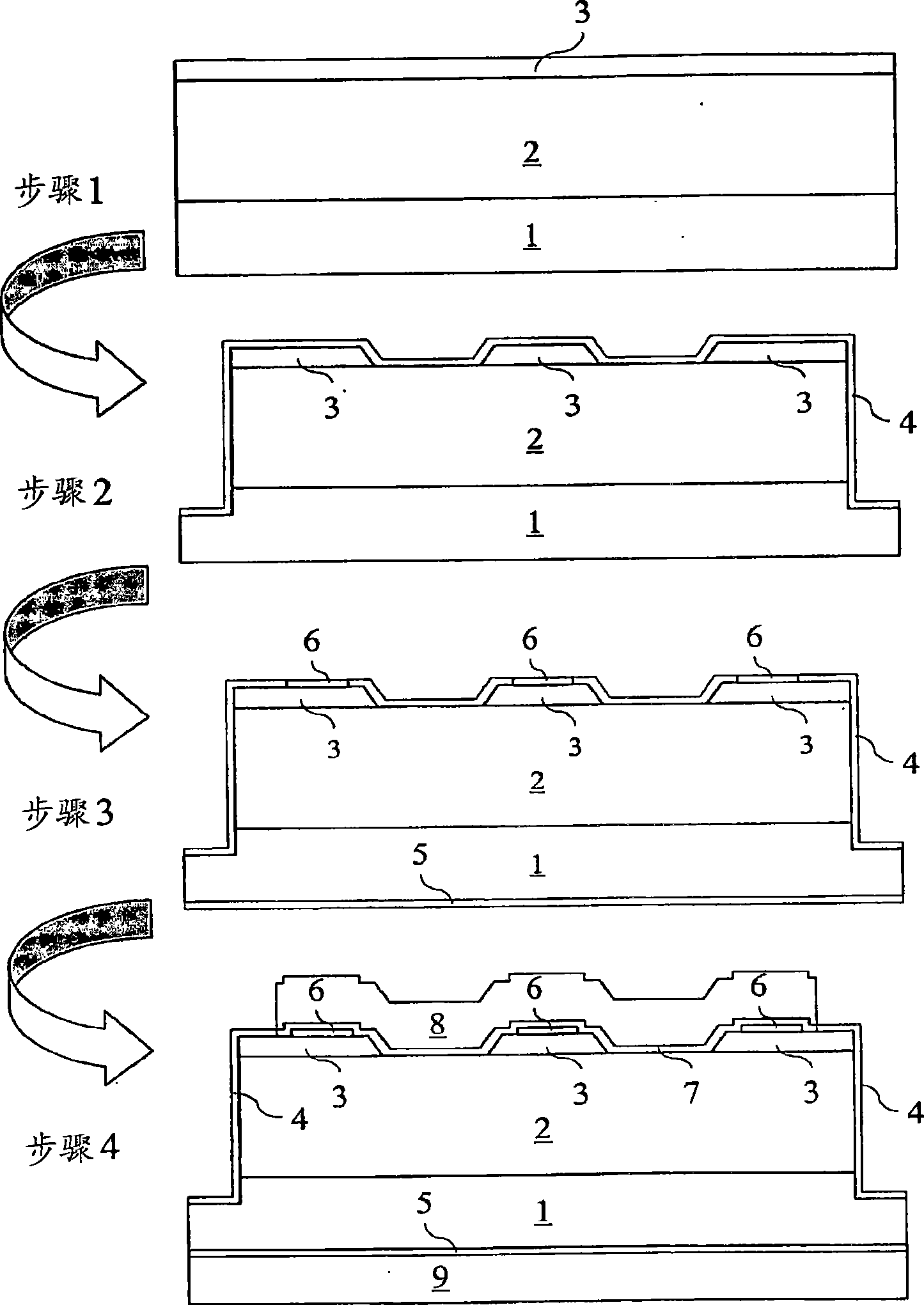
[0046] According to one embodiment, the device includes a monolithically integrated Schottky barrier diode and a p-type / intrinsic / n-type (PiN) junction diode connected in parallel. figure 1Exemplary devices are shown. Under normal operating conditions, the device acts as a Schottky barrier diode with most of the current flowing through the Schottky contact. However, under surge current conditions, the current mainly flows through the p-n junction due to the significant decrease in drift resistance due to conductance modulation at larger current densities. This phenomenon can be explained by the following mathematical formula, which calculates the forward current density J F The specific resistance of the base region of the PiN diode (Reference 6):

[0047] R ( J F ) = t q · μ n ...


PUM

PropertyMeasurementUnit
Doping concentrationaaaaaaaaaa
Thicknessaaaaaaaaaa
Doping concentrationaaaaaaaaaa

Abstract

The present invention provides a wide bandgap semiconductor device with surge current protection and a method of making the device. The device comprises a low doped n-type region formed by plasma etching through the first epitaxial layer grown on a heavily doped n-type substrate and a plurality of heavily doped p-type regions formed by plasma etching through the second epitaxial layer grown on the first epitaxial layer. Ohmic contacts are formed on p-type regions and on the backside of the n-type substrate. Schottky contacts are formed on the top surface of the n-type region. At normal operating conditions, the current in the device flows through the Schottky contacts. The device, however, is capable of withstanding extremely high current densities due to conductivity modulation caused by minority carrier injection from p-type regions.

Description

[0001] Statement Regarding Federally Funded Research [0002] This invention was made under US Government Awarded Contract No. F33615-02-D-2103 awarded by the US Air Force. The United States Government may have certain rights in this invention. technical field [0003] The present invention relates generally to semiconductor devices of wide bandgap semiconductor materials, and in particular to diodes (including Schottky barrier diodes and bipolar junction diodes) fabricated in silicon carbide (SiC), and to monolithically integrating these diodes structures, including structures with mesa edge terminations. Background technique [0004] Monolithic devices including Schottky and PiN diodes are known (eg, see US Patent No. 6,861,723 and Document 1). U.S. Patent No. 6,573,128 discloses a SiC junction barrier Schottky (JBS) / merged P-I-N Schottky (MPS) gate consisting of p-type islands defined by plasma etching through epitaxially grown layers. Deposited Schottky metal formatio...

Claims


Application Information

Patent Timeline
IPC IPC(8): H01L29/872H01L29/868
CPCH01L29/872H01L29/1608H01L29/868H01L29/0619Y02E10/548H01L29/47H01L29/812
Inventor 伊格尔·桑金约瑟夫·尼尔·梅里特
Owner PI
Why Eureka
Try Eureka