Printed circuit boards with stacked micros vias

A printed circuit board, circuit board technology, applied in the direction of printed circuit, printed circuit, printed circuit manufacturing, etc., can solve the problems of expensive, difficult to achieve rapid change, time-consuming processing sequence, etc.

Active Publication Date: 2009-06-03
DYNAMIC DETAILS
View PDF0 Cites 15 Cited by
  • Summary
  • Abstract
  • Description
  • Claims
  • Application Information

AI Technical Summary

Problems solved by technology

[0005] Additionally, plating through-holes (or vias) with copper materials requires additi

Method used


Image

  • Printed circuit boards with stacked micros vias
  • Printed circuit boards with stacked micros vias
  • Printed circuit boards with stacked micros vias

Examples


Embodiment Construction

[0046] In the following detailed description, there are shown and described, by way of illustration, certain exemplary embodiments of the invention. As those skilled in the art would realize, the described exemplary embodiment may be modified in various different ways, all without departing from the spirit and scope of the present invention. Accordingly, the drawings and descriptions are to be regarded as illustrative in nature and not restrictive. Parts shown in the drawings, or parts not shown in the drawings, which are not discussed in the specification, are not considered indispensable to a complete understanding of the invention. The same reference numerals denote the same elements.

[0047] first exemplary embodiment

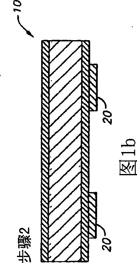
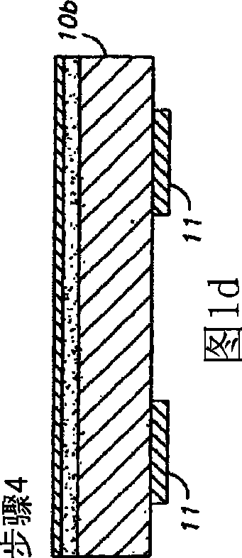
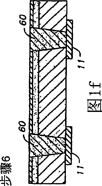
[0048] A method of manufacturing a printed circuit board according to a first exemplary embodiment of the present invention, utilizing a single lamination cycle or a processing sequence with stacked (or staggered) microvias, will be described with refere...


PUM


Abstract

The present invention provides printed circuit boards having circuit layers laminated with stacked (or staggered) micro via(s) and methods of manufacturing the same. Aspects of embodiments of the present invention are directed to a printed circuit board with Z-axis interconnect(s) or micro via(s) that can eliminate a need for plating micro vias and/or eliminate a need for planarizing plated bumps of a surface, that can be fabricated with one or two lamination cycles, and/or that can have carrier-to-carrier (or substrate-to-substrate) attachments with conductive vias, each filled with a conductive material (e.g., with a conductive paste) in the Z-axis. In one embodiment, a printed circuit board having a plurality of circuit layers with at least one z-axis interconnect can be fabricated using a single lamination cycle.

Description

[0001] Cross-Referenced Related Applications [0002] This application claims priority from US Patent Application No. 11 / 706,473, filed February 14, 2007, and US Provisional Application No. 60 / 793,370, filed April 19, 2006. field of invention [0003] The present invention relates generally to printed circuit boards and methods of making the same, and more particularly to printed circuit boards having laminated circuit layers with stacked (staggered) microvias and methods of making the same. Background technique [0004] Most electronic systems include printed circuit boards with high density electrical interconnections. A printed circuit board includes one or more circuit cores, a substrate, or a carrier. In a fabrication scheme for printed circuit boards having one or more circuit carriers, electronic circuits (i.e., pads, electrical interconnections, etc.) are formed on opposite sides of a circuit carrier to form a pair of circuit layer. The resulting circuit board str...

Claims


Application Information

Patent Timeline
IPC IPC(8): H05K1/00H05K1/03H05K1/16B32B3/00B32B15/08
CPCH05K2201/09309H05K3/386H05K2203/061H05K3/205H05K3/4617H05K2201/0355H05K3/4069H05K2203/0733H05K2203/1461H05K3/4614H05K3/423H05K2203/1536H05K2203/0191H05K3/4623H05K3/462H05K2201/0394H05K2201/096H05K2203/0271H05K2203/0502H05K2203/107H05K2203/304Y10T29/49126Y10T29/49155Y10T29/49165
Inventor 拉伊.·库梅尔蒙特·德雷尔迈克尔·J·泰勒
Owner DYNAMIC DETAILS
Why Eureka
Try Eureka