
OTP construction and manufacturing method thereof

A technology of silicon oxide layer and silicon oxide, which is applied in semiconductor/solid-state device manufacturing, electrical components, electric solid-state devices, etc., can solve the problems that the OTP structure cannot meet the high-density storage function, and achieve area saving, production cost reduction, and improved The Effect of Storage Density

Inactive Publication Date: 2009-06-10
SHANGHAI HUA HONG NEC ELECTRONICS
View PDF0 Cites 2 Cited by
  • Summary
  • Abstract
  • Description
  • Claims
  • Application Information

AI Technical Summary

Problems solved by technology

[0003] As the integration level of the semiconductor industry becomes higher and higher, and the volume of semiconductor devices becomes smaller, the storage density of the storage unit is also required to increase. The existing OTP structure, which can only store one bit of data in a unit structure, cannot meet this high-density storage. Function

Method used


Image

  • OTP construction and manufacturing method thereof
  • OTP construction and manufacturing method thereof
  • OTP construction and manufacturing method thereof

Examples


Embodiment Construction

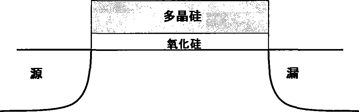
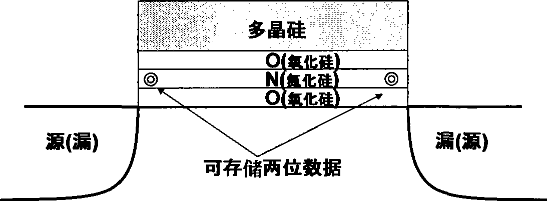
[0015] Such as figure 1 As shown, the OTP structure of the present invention includes a substrate, and the top of the substrate is successively silicon oxide-silicon nitride-silicon oxide layer and polysilicon layer, and the two sides of the polysilicon on the substrate are respectively a source electrode and a drain electrode, wherein silicon oxide-silicon oxide layer The thickness of the silicon oxide layer on both sides of the silicon nitride-silicon oxide layer is greater than 50 Angstroms.

[0016] When writing data to the OTP structure of the present invention, electrons will be trapped in the nitride layer of silicon oxide-silicon nitride-silicon oxide layer and not easy to move. When the potential is high, hot electron injection occurs on the side near the drain end, and write electrons are stored on the side of the silicon oxide-silicon nitride-silicon oxide layer. When a high potential is applied to the source terminal and a low potential is applied to the drain, ho...


PUM

PropertyMeasurementUnit
Thicknessaaaaaaaaaa

Abstract

The invention discloses an OTP structure. A silicon oxide-silicon nitride-silicon oxide layer and a polycrystalline silicon layer of a transistor part are orderly arranged on a substrate, and both sides of the polycrystalline silicon on the substrate are provided with a source electrode and a drain electrode respectively. In order to prepare the OTP structure, the invention also discloses a method for preparing the OTP structure, which comprises the following steps: 1, active region isolation; 2, well injection; 3, silicon oxide-silicon nitride-silicon oxide layer sedimentation and etching; 4, gate oxygen growth and etching; 5, light doping injection and source-drain injection; and 6, OTP injection. The OPT structure prepared by the method has the advantages that two electrons can be stored in one OTP structure, thereby realizing the effect of two-bit storage in each cell structure, improving storage density of the storage cell, reducing areas of a chip and lowering production cost.

Description

technical field [0001] The invention relates to the technical field of semiconductors, in particular to an OTP structure in the semiconductor field and a manufacturing method thereof. Background technique [0002] OTP is a commonly used memory unit in the semiconductor industry, such as figure 1 As shown, in the existing OTP structure, a silicon oxide layer and a polysilicon layer are sequentially formed above the substrate, and source electrodes and drain electrodes are respectively formed on both sides of the substrate. In this existing OTP structure, memory charges are generally stored on polysilicon floating gates, electrons can move freely on the floating gates, and a cell structure can only store one bit of data. The magnitude of the threshold voltage is used to judge whether there are injected electrons on the floating gate, and 0 or 1 is represented in a unit. [0003] As the integration level of the semiconductor industry becomes higher and higher, and the volume ...

Claims


Application Information

Patent Timeline
IPC IPC(8): H01L27/115H01L29/78H01L29/51H01L29/423H01L21/8247H01L21/336
Inventor 戚丽娜
Owner SHANGHAI HUA HONG NEC ELECTRONICS
Features
  • Generate Ideas
  • Intellectual Property
  • Life Sciences
  • Materials
  • Tech Scout
  • Unparalleled Data Quality
  • Higher Quality Content
  • 60% Fewer Hallucinations
Learn More