Solar battery and method for manufacturing the same

A solar cell and electrode technology, which is applied in the field of solar cells, can solve problems such as insufficient sunlight absorption and negative effects on efficiency, and achieve the effects of improving optical absorption properties, reducing the minimum, and improving the photodegradation of amorphous silicon

Inactive Publication Date: 2009-06-17
DELTA ELECTRONICS INC +1
View PDF0 Cites 9 Cited by
  • Summary
  • Abstract
  • Description
  • Claims
  • Application Information

AI Technical Summary

Problems solved by technology

However, thinning the film thickness below the minimum absorption thickness will result in insufficient sunlight absorption and negatively impact efficiency

Method used


Image

  • Solar battery and method for manufacturing the same
  • Solar battery and method for manufacturing the same
  • Solar battery and method for manufacturing the same

Examples


Embodiment Construction

[0032] A solar cell and a manufacturing method thereof according to preferred embodiments of the present invention will be described below with reference to related drawings.

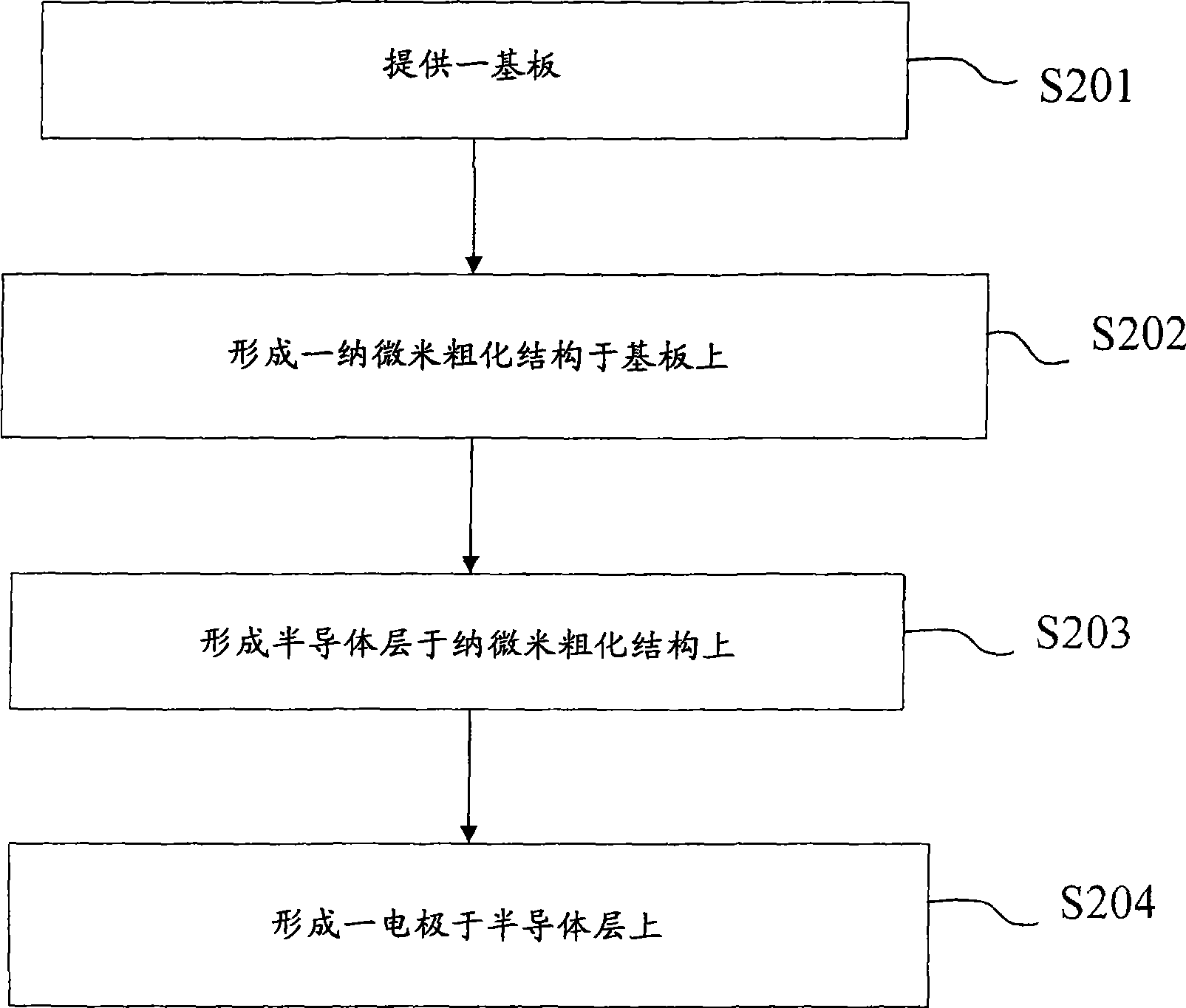
[0033] figure 2 It is a flowchart of a method for fabricating a solar cell according to an embodiment of the present invention. Figure 3A to Figure 3D for figure 2 Cross-section diagrams for each step.

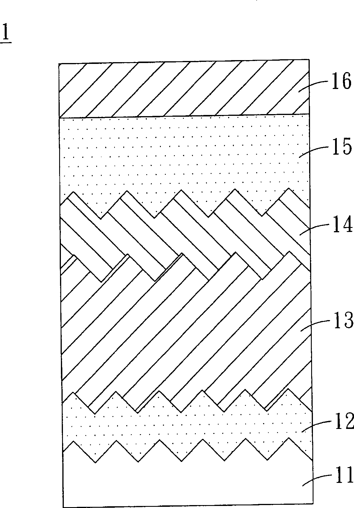
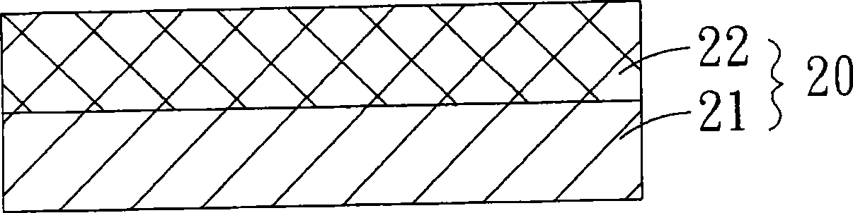
[0034] First, if Figure 3A As shown, a substrate 20 is provided, which is a transparent substrate 21 having a first transparent conductive layer 22 (step S201 ). The transparent substrate 21 can be a glass substrate, but not limited thereto. The first transparent conductive layer 22 is a transparent conductive oxide film (Transparent Conductive Oxide, TCO), such as indium tin oxide (Indium Tin Oxide, ITO), but This is not the limit. In addition, the surface of the first transparent conductive layer 22 has a rough (textured) or smooth (smooth) surface structure.

[0035] Next, if Figure 3B As...


PUM


Abstract

The invention provides a solar cell and a manufacturing method thereof, the solar cell comprises a substrate, a nano-micron coarsening structure and a semiconductor layer, wherein the substrate is provided a first transparent conducting layer, the nano-micron coarsening structure is formed on the first transparent conducting layer, and the semiconductor layer is formed on the nano-micron coarsening structure and is coated on the nano-micron coarsening structure.

Description

technical field [0001] The invention relates to a solar cell device and a manufacturing method thereof, in particular to a solar cell in which a nano-micron roughened structure is formed between a substrate and a semiconductor layer, so as to improve the photoelectric conversion efficiency of the solar cell. Background technique [0002] At present, the mainstream of solar cells is silicon wafer solar cells, accounting for about 90% of the total output. However, in recent years, the shortage of silicon raw materials has drawn attention to thin-film solar cells that do not require the use of silicon raw materials or can reduce the amount of silicon used. The current development of solar cells is still dominated by silicon-based solar cells. In order to pursue the effective absorption and utilization of the solar spectrum, stacked solar cells (Tandem cells) are currently the development axis of silicon thin film solar cells. [0003] figure 1 It is a schematic diagram of a k...

Claims


Application Information

Patent Timeline
Patent Type & Authority Applications(China)
IPC IPC(8): H01L31/042H01L31/0236H01L31/18
CPCY02E10/50
Inventor 陈启昌詹佳桦吴皇南姚富渊陈升晖谢宏健李正中邢泰刚
Owner DELTA ELECTRONICS INC
Why Eureka
Try Eureka