

High-power semiconductor laser beam composite apparatus
A compound device and laser beam technology, which is applied in the laser field, can solve the problems of increasing cost, damaging the polarization beam combiner, and the relatively high damage energy threshold of the polarization beam combiner, and achieve the effect of reducing volume and weight and reducing cost
- Summary
- Abstract
- Description
- Claims
- Application Information
AI Technical Summary
Problems solved by technology
Method used
Image

Examples
Embodiment 1
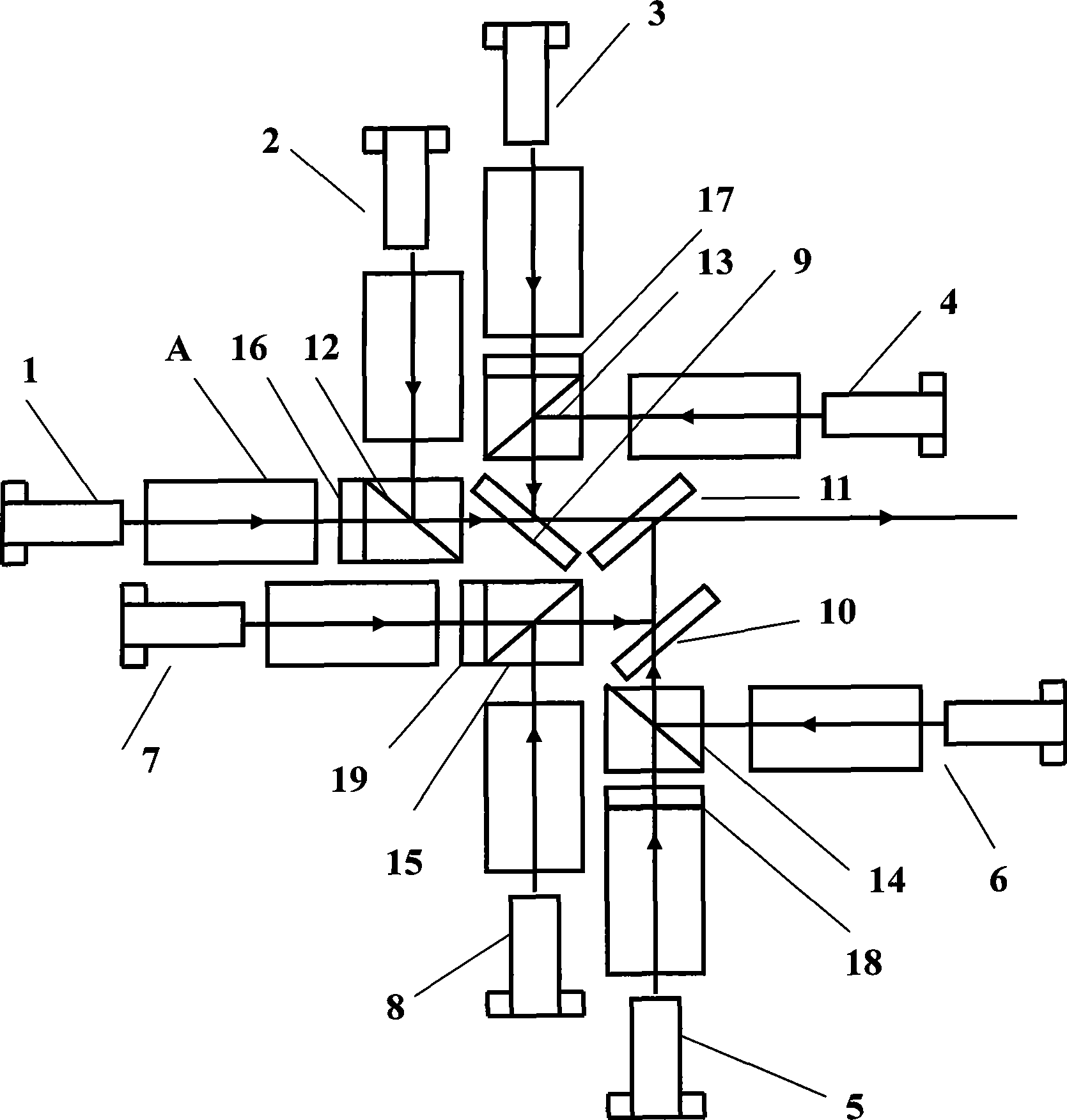
[0023] The structure of this embodiment is as figure 1 As shown, including the first semiconductor laser array 1, the second semiconductor laser array 2, the third semiconductor laser array 3, the fourth semiconductor laser array 4, the fifth semiconductor laser array 5, the sixth semiconductor laser array 6, the seventh semiconductor laser array Array 7, the eighth semiconductor laser array 8, and the first wavelength combiner 9, the second wavelength combiner 10, the third wavelength combiner 11, the first polarization beam combiner 12, the second polarization beam combiner 13 , a third polarization beam combiner 14, a fourth polarization beam combiner 15, a first wave plate 16, a second wave plate 17, a third wave plate 18, a fourth wave plate 19 and eight shaping devices A. The eight semiconductor laser arrays in this embodiment all output P-state light or S-state light.
[0024] The light emitted by the first semiconductor laser array 1 after beam shaping passes through ...
Embodiment 2
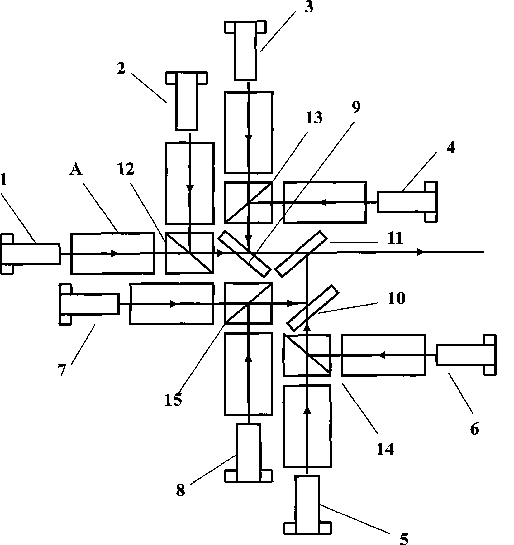
[0026] This example figure 2 As shown, the difference between it and Embodiment 1 is that the first semiconductor laser array 1, the third semiconductor laser array 3, the fifth semiconductor laser array 5 and the seventh semiconductor laser array 7 output S-state light, the second semiconductor laser array 2, The fourth semiconductor laser array 4, the sixth semiconductor laser array 6 and the eighth semiconductor laser array 8 output P-state light, so the first wave plate, the second wave plate 17, the third wave plate 18 and the first wave plate are not needed in this embodiment. Four wave plates 19 to change the polarization state. Other structures are the same as in Embodiment 1.
Embodiment 3
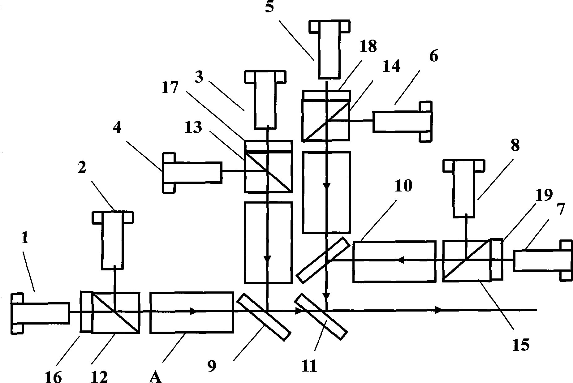
[0028] The structure of this embodiment is as image 3 As shown, including the first semiconductor laser array 1, the second semiconductor laser array 2, the third semiconductor laser array 3, the fourth semiconductor laser array 4, the fifth semiconductor laser array 5, the sixth semiconductor laser array 6, the seventh semiconductor laser array Array 7, the eighth semiconductor laser array 8, and the first wavelength combiner 9, the second wavelength combiner 10, the third wavelength combiner 11, the first polarization beam combiner 12, the second polarization beam combiner 13 , a third polarization beam combiner 14, a fourth polarization beam combiner, a first wave plate 16, a second wave plate 17, a third wave plate 18, a fourth wave plate 19 and four shaping devices A. The eight semiconductor laser arrays in this embodiment all output P-state light or S-state light.
[0029] The difference between this embodiment and Embodiment 1 is that in this embodiment, the light emi...
PUM
 Abstract
Description
Claims
Application Information