
Method for producing single-layer polysilicon gate non-volatile memory

A single-layer polysilicon, non-volatile technology, applied in the manufacture of electric solid-state devices, semiconductor devices, semiconductor/solid-state devices, etc., can solve the problems of poor charge storage performance and high mobile ion concentration of single-layer polysilicon gate memory, and achieve improvement Charge storage performance, moderate temperature effect

Inactive Publication Date: 2009-08-05
SEMICON MFG INT (SHANGHAI) CORP
View PDF0 Cites 2 Cited by
  • Summary
  • Abstract
  • Description
  • Claims
  • Application Information

AI Technical Summary

Problems solved by technology

[0005] The disadvantage of the single-layer polysilicon gate memory relative to the double-layer polysilicon gate memory is that the charge storage performance of the single-layer polysilicon gate memory is relatively poor, that is, the concentration of positive mobile ions in the silicon gate is relatively high. How to solve this problem Critical to the application of the single polysilicon gate non-volatile memory

Method used


Image

  • Method for producing single-layer polysilicon gate non-volatile memory
  • Method for producing single-layer polysilicon gate non-volatile memory
  • Method for producing single-layer polysilicon gate non-volatile memory

Examples


Embodiment 1

[0019] Using the same prior art (including prior art methods and materials used in the prior art) to complete the partial structure of the single-layer polysilicon gate memory cell, including the following steps:

[0020] 1 Form an isolation region on a P-type silicon substrate;

[0021] 2 Photolithography to form the N-well pattern as the control gate, and perform N-well ion implantation;

[0022] 3 Form gate oxide layer and undoped polysilicon gate in sequence;

[0023] 4 Perform lightly doped drain (LDD) implantation;

[0024] 5 forming a protective layer on the gate side;

[0025] 6 Form contact holes.

[0026] Afterwards, use the method of low pressure vapor phase chemical deposition (the method of low pressure chemical vapor deposition here is the same as the growth method of LPTEOS film layer in the prior art) TEOS, grow The thickness of the LPTEOS film layer is used as the SAB layer, replacing the existing technology Thickness of the SRO film layer, as the SAB l...

Embodiment 2

[0033] In this embodiment, after the step 6 in the embodiment 1, the following method is used to manufacture the SAB layer:

[0034] At first, use the method of low pressure vapor phase chemical deposition (the method of low pressure chemical vapor deposition here is the same as the growth method of LPTEOS film layer in the prior art), grow The first low pressure chemical vapor deposition orthosilicate film layer (also can be called the first LPTEOS film layer) of thickness; The method of growing the silicon nitride film layer by the low pressure chemical vapor deposition method is the same) Thick silicon nitride film layer; Finally, use the method of low pressure vapor phase chemical deposition (the method of low pressure chemical vapor phase deposition here is the same as the growth method of LPTEOS film layer in the prior art), grow The thickness of the second low-pressure chemical vapor deposition tetraethyl silicate film layer (also called the second LPTEOS film layer...


PUM


Abstract

The invention relates to a method for improving the performance of a single-layer polysilicon gate nonvolatile memory. By changing the materials of an SAB (Salicide-Block) layer, the number of positive movable ions entering the floating gate of a single-layer polysilicon gate nonvolatile memory unit can be decreased, so the charge retention of a storage unit is enhanced.

Description

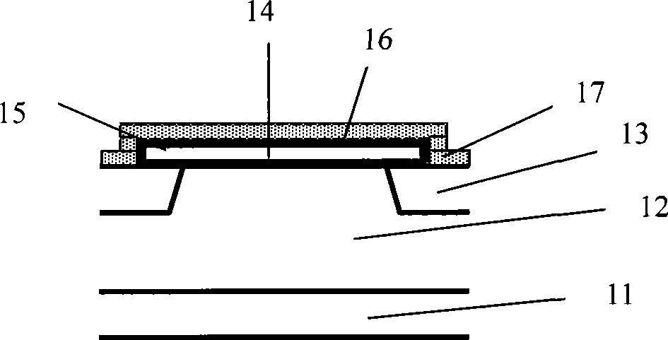
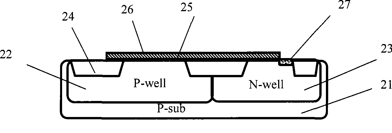
technical field [0001] The invention relates to a method for preparing a single-layer polysilicon gate non-volatile memory. Background technique [0002] A key feature of non-volatile memory technology is the widespread use of floating-gate cells, such as EEPROM. According to different gate structures, floating gate units can be divided into two types, one is the so-called stacked gate (ie double-layer polysilicon gate) structure, such as figure 1 As shown, it includes: P-type silicon substrate 11, P-well 12, shallow trench isolation 13, gate oxide layer 14, floating gate 15, inner layer isolation layer 16, and control gate 17 stacked above the floating gate 15; Single-layer polysilicon gate structure, such as figure 2 As shown, it includes: P-type silicon substrate 21 , P-well 22 , N-well 23 , shallow trench isolation 24 , gate oxide layer 25 , floating gate 26 and highly doped contact region 27 . In a single polysilicon gate memory cell, the N-well 23 functions as a co...

Claims


Application Information

Patent Timeline
Patent Type & Authority Applications(China)
IPC IPC(8): H01L21/00H01L21/336H01L21/8247H01L21/31H01L29/78H01L27/115H10B69/00
Inventor 金起凖崔崟郭兵梅奎程超
Owner SEMICON MFG INT (SHANGHAI) CORP
Learn More