Image element structure of thin-film transistor LCD array substrates
A liquid crystal display and thin film transistor technology, applied in the field of pixel structure, can solve the problems that the parasitic capacitance part does not provide any protection measures, affects the quality and yield, and the DGS line is defective, so as to reduce the rate of defective lines, increase costs, and reduce The effect of production costs
- Summary
- Abstract
- Description
- Claims
- Application Information
AI Technical Summary
Problems solved by technology
Method used
Image


Examples
Embodiment 1
[0023] This embodiment provides a pixel unit of a TFT-LCD array substrate, and the pixel structure is manufactured by five masking processes. The five-time mask process is an existing pixel structure manufacturing method. Its main process includes:
[0024] 1. Forming gate lines, gate line branches and gates on the substrate 00 through film formation, exposure, and etching processes;
[0025] 2. Deposit the first protective layer directly, and form the active layer pattern through film formation, exposure, and etching processes;
[0026] 3. Form data lines, source electrodes and drain electrodes through film formation, exposure, and etching processes;
[0027] 4. Form via holes through film formation, exposure, and etching processes;
[0028] 5. A pixel electrode is formed through film formation, exposure, and etching processes, and the pixel electrode is connected to the source through a via hole.
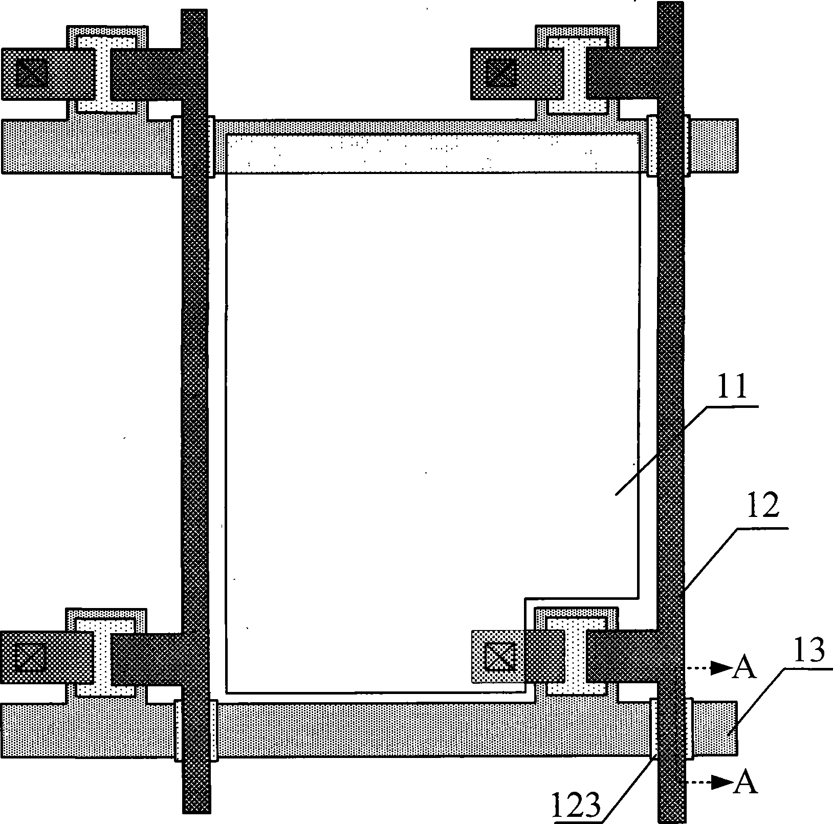
[0029] like Figure 3A As shown, the pixel structure described in this e...
Embodiment 2
[0037] This embodiment provides another pixel structure of a TFT-LCD array substrate, which is manufactured by four masking processes. The four-time mask process is also an existing pixel structure manufacturing method. Its main process includes:
[0038] 1. Forming the gate wire and the extension of the gate wire and the gate on the substrate 00 through film formation, exposure, and etching processes;
[0039] 2. Deposit the first protective layer directly, and form active layer patterns, data lines, source electrodes and drain electrodes through film formation, exposure, and etching processes;
[0040] 3. Via holes are formed through film formation, exposure, and etching processes;
[0041] 4. Forming the pixel electrode and the lead part through film formation, exposure and etching processes, wherein the pixel electrode is connected to the source through the via hole, and the lead part is connected to the extension part of the gate line through the via hole.
[0042] lik...
PUM
 Abstract
Description
Claims
Application Information
 - R&D
- Intellectual Property
- Life Sciences
- Materials
- Tech Scout
- Unparalleled Data Quality
- Higher Quality Content
- 60% Fewer Hallucinations
Browse by: Latest US Patents, China's latest patents, Technical Efficacy Thesaurus, Application Domain, Technology Topic, Popular Technical Reports.
© 2025 PatSnap. All rights reserved.Legal|Privacy policy|Modern Slavery Act Transparency Statement|Sitemap|About US| Contact US: help@patsnap.com