

Method for measuring surface charge density of materials
A technology of surface charge density and surface topography, which is applied in the field of surface analysis, can solve problems such as complex charge density, and achieve the effect of simple measurement and easy operation
- Summary
- Abstract
- Description
- Claims
- Application Information
AI Technical Summary
Problems solved by technology
Method used
Image

Examples
Embodiment Construction
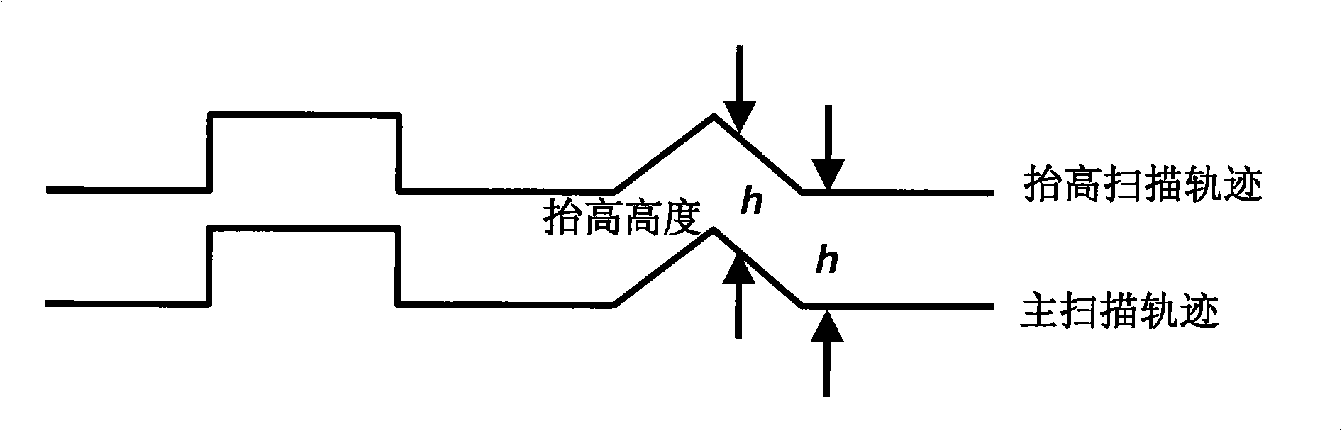
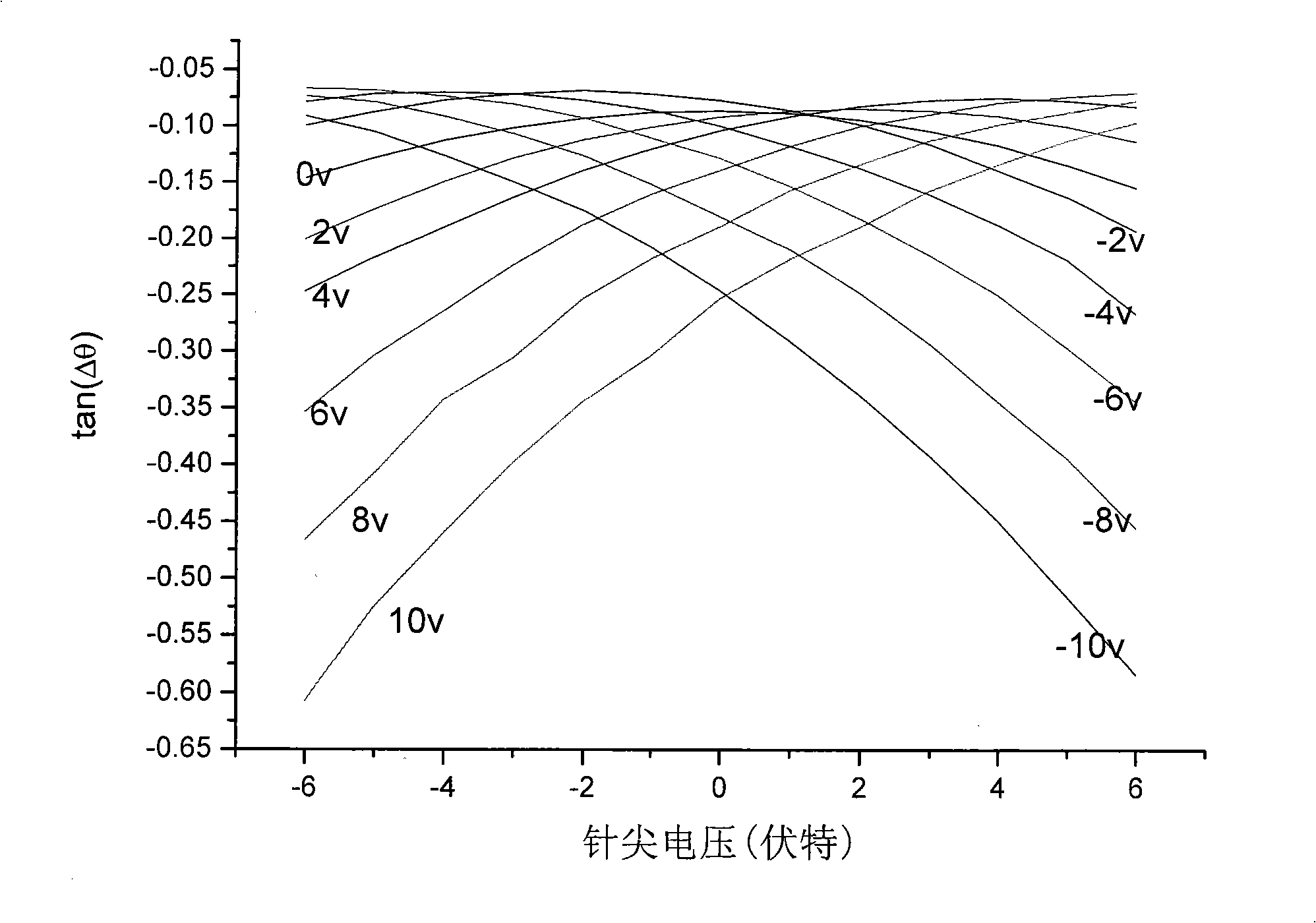
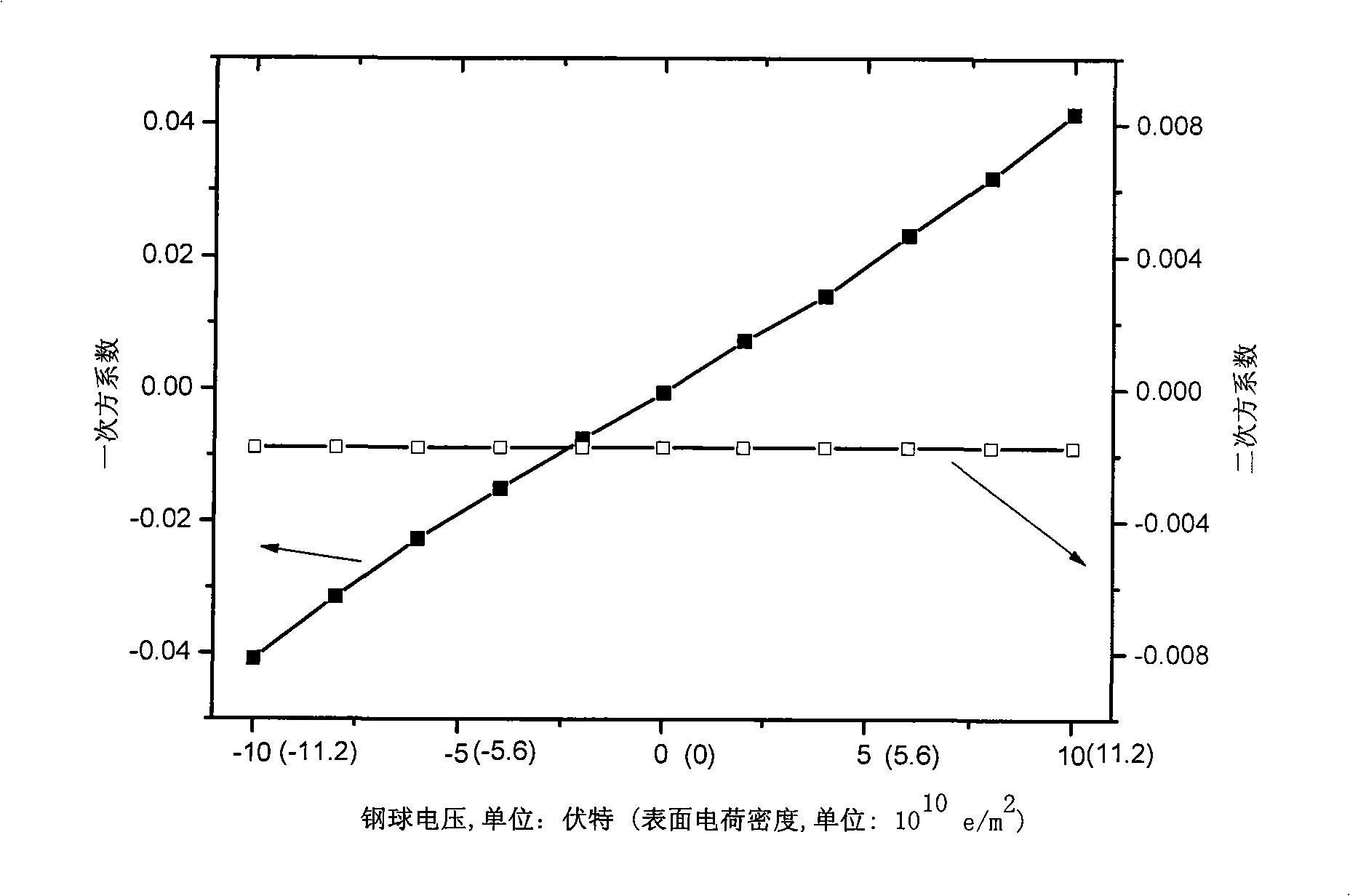
[0028] The present invention is based on the CSPM method for measuring the surface charge density of a sample, and describes the relationship between the phase change of the CSPM conductive tip vibration and the tip bias voltage under the action of a series of steel ball model biases. The relational formula includes the sample surface charge density and The relationship between tip bias voltage. During the scanning process in the elevation mode, the force between the needle tip and the sample mainly comes from three parts: the force generated by the capacitive interaction between the needle tip and the sample; the force between the charged charge on the needle tip and the surface charge density of the sample; The force between the charge on the surface and the image charge on the tip of the sample surface.
[0029] In elevated mode, the total electrostatic force acting on the cantilever can be expressed as:
[0030] F = 1 2...
PUM
| Property | Measurement | Unit |
|---|---|---|
| Diameter | aaaaa | aaaaa |
Abstract
Description
Claims
Application Information