

Method for testing the stress of side wall of field effect transistor
A field-effect transistor and sidewall technology, which is applied in the field of testing field-effect transistor sidewall stress, can solve problems such as troublesome design and different threshold voltages of transistors, achieve high realizability, and solve the effect of timely detection of sidewall quality
- Summary
- Abstract
- Description
- Claims
- Application Information
AI Technical Summary
Problems solved by technology
Method used
Image

Examples
Embodiment Construction
[0026] The preferred embodiment of the present invention is described in more detail below with reference to the accompanying drawings of the present invention.
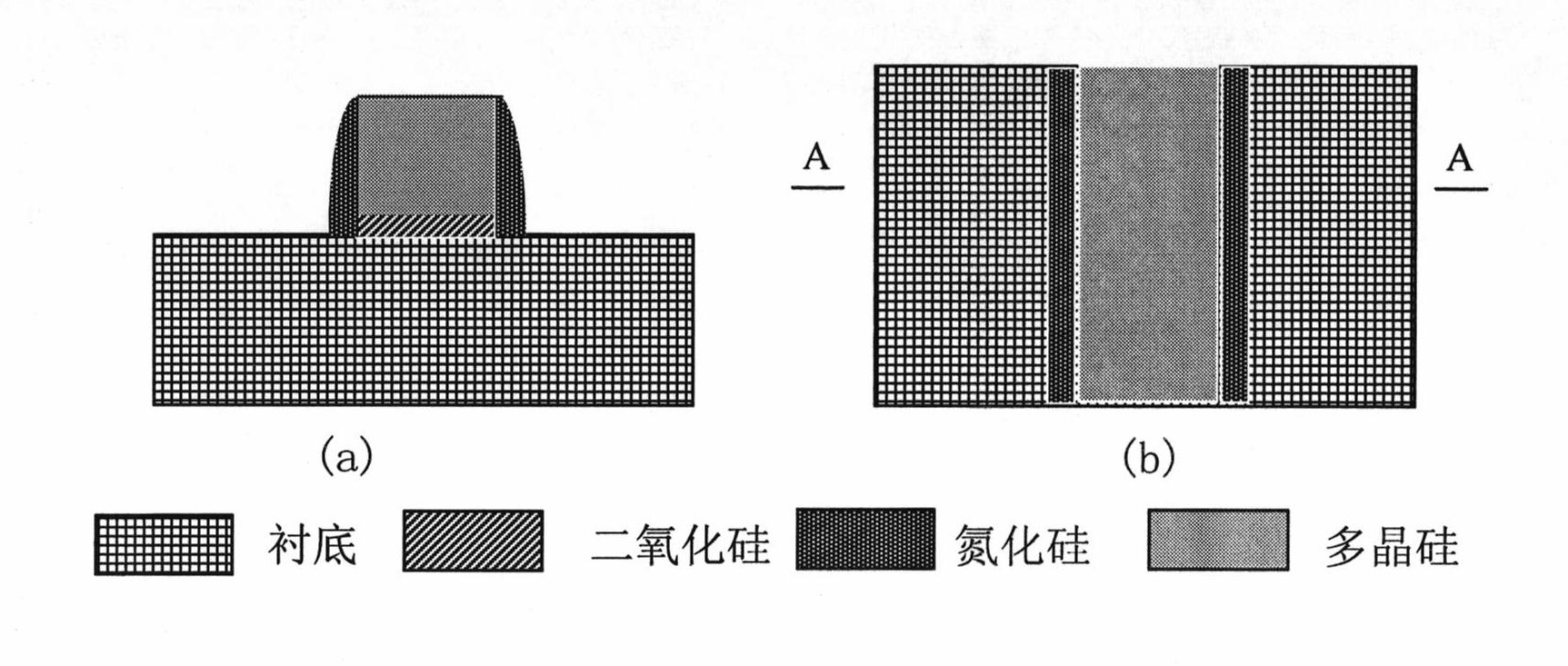
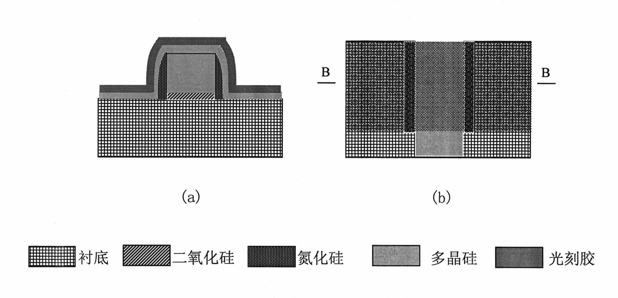
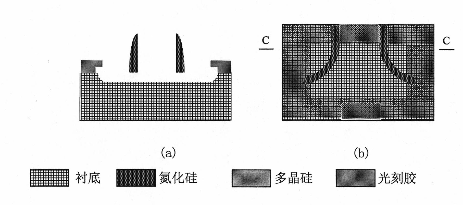
[0027] 1. Taking the silicon nitride sidewall as an example to illustrate the test method of the transistor sidewall stress of the present invention, the specific test steps are as follows:
[0028] 1. Form a gate structure.
[0029] Use low-pressure chemical vapor deposition (LPCVD) to grow silicon dioxide 20nm and polysilicon 480nm on the substrate silicon, then use photolithography to define the gate area, and use anisotropic reactive ion etching (RIE) to etch the non-gate area polysilicon 480nm and 480nm polysilicon The silicon dioxide is 20nm, and a 500nm step structure is formed on the substrate silicon wafer.
[0030] 2. Form side walls.
[0031] Using low-pressure chemical vapor deposition (LPCVD) 50nm silicon nitride and anisotropic reactive ion etching (RIE) 50nm silicon nitride, silicon nitride sidewalls...
PUM
| Property | Measurement | Unit |
|---|---|---|
| width | aaaaa | aaaaa |
Abstract
Description
Claims
Application Information