

Beam shaping illumination system of semiconductor laser array
A laser array and beam shaping technology, which is applied to semiconductor laser devices, semiconductor devices of light-emitting elements, laser devices, etc., can solve problems such as low efficiency, high production cost, and difficulty in integration
Inactive Publication Date: 2011-01-05
ZHEJIANG UNIV
View PDF0 Cites 0 Cited by
- Summary
- Abstract
- Description
- Claims
- Application Information
AI Technical Summary
Problems solved by technology
In order to overcome the shortcomings of the existing semiconductor laser array beam shaping lighting system, such as low efficiency, complex structure, difficult integration, and high production cost, the purpose of the present invention is to provide a semiconductor laser array beam shaping lighting system, which can significantly Improve the light energy utilization efficiency of laser lighting, and has the characteristics of simple structure, low production cost and the integration of multiple modules to achieve ultra-high power lighting
Method used
View moreImage
Smart ImageViewing Examples

Examples
Embodiment 1
Embodiment 2
Embodiment 3
Login to View More PUM
 Abstract
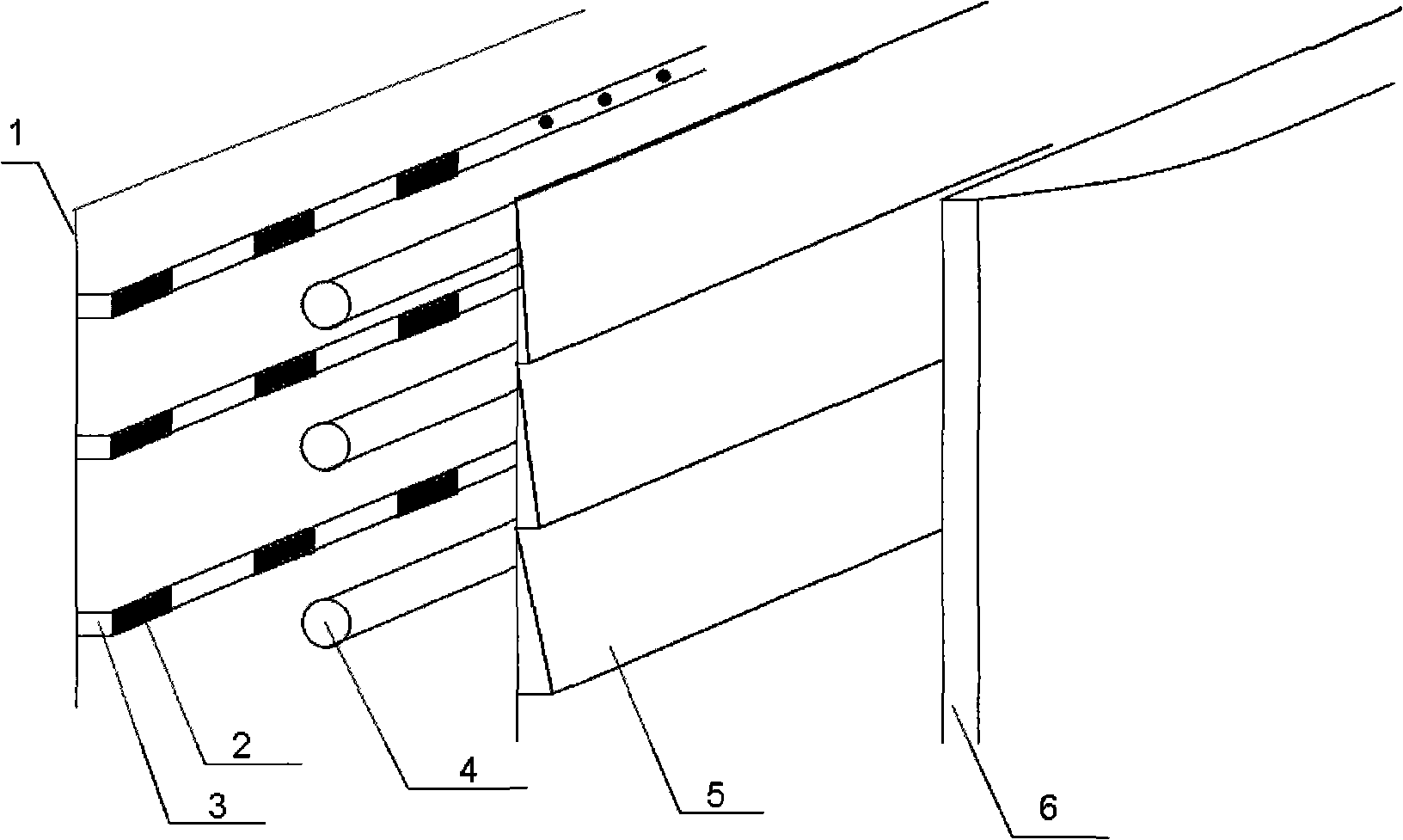
The invention discloses a beam shaping illumination system of a semiconductor laser array, which comprises the semiconductor laser array, an optical system for transforming beam divergence angles of a fast axis, a device for deflecting angles of beams in the fast axis direction, and an optical system for transforming divergence angles of a slow axis and deflecting the beams in the slow axis direction. The system has a key point that the superposition effect of Gaussian beam parts of a plurality of laser units is formed in a distant field by controlling the deflection degree of beam transmission axes of each laser unit in the fast axis and slow axis directions respectively so as to construct illumination beams according with field coverage requirements. The system has the characteristics of high efficiency, simple structure, low cost, integration and practicability, and is particularly applicable as an illumination light source of area array imaging laser radar and active laser illumination detecting systems.
Description
Semiconductor laser array beam shaping illumination system technical field The invention relates to a light beam shaping illumination system of a semiconductor laser array. Background technique In order to obtain integrated high-power output, the semiconductor laser array uses a semiconductor laser output module composed of semiconductor laser units in a series-parallel form. It has the characteristics of high output power, high photoelectric conversion efficiency, convenient laser intensity modulation, small size, and long life. It is very suitable for As an active illumination source for area array imaging lidar and laser detection systems. Semiconductor lasers have a special resonator structure and working mode, which makes the spatial distribution of the beam asymmetrical, with a divergence angle of about 40 degrees in the direction perpendicular to the junction plane (fast axis direction), and a divergence angle of about 40 degrees in the direction parallel to the ju...
Claims
Login to View More Application Information
Patent Timeline
 Patent Type & AuthorityPatents(China)
IPC IPC(8): G02B27/09G02F1/01F21K7/00H01S5/40F21V5/00F21K99/00F21K9/20F21Y115/30
Inventor严惠民姜燕冰张秀达
OwnerZHEJIANG UNIV