Method for manufacturing an electronic module and an electronic module

A technology of electronic modules and conductive patterns, which is applied to printed circuits connected with non-printed electrical components, printed circuit manufacturing, multilayer circuit manufacturing, etc., can solve complex problems, improve characteristics, reduce loss, and improve long-term stability sexual effect

Active Publication Date: 2009-09-30
IMBERATEK LLC
View PDF3 Cites 5 Cited by
  • Summary
  • Abstract
  • Description
  • Claims
  • Application Information

AI Technical Summary

Problems solved by technology

If one wishes to make a mechanically durable structure, the device must also be attached to the mounting base, so this approach is quite complex
There are great difficulties in employing complex methods requiring several different materials and process steps in order to advantageously manufacture inexpensive articles

Method used


Image

  • Method for manufacturing an electronic module and an electronic module
  • Method for manufacturing an electronic module and an electronic module
  • Method for manufacturing an electronic module and an electronic module

Examples


Embodiment Construction

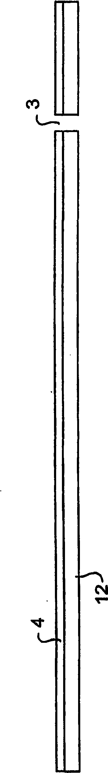
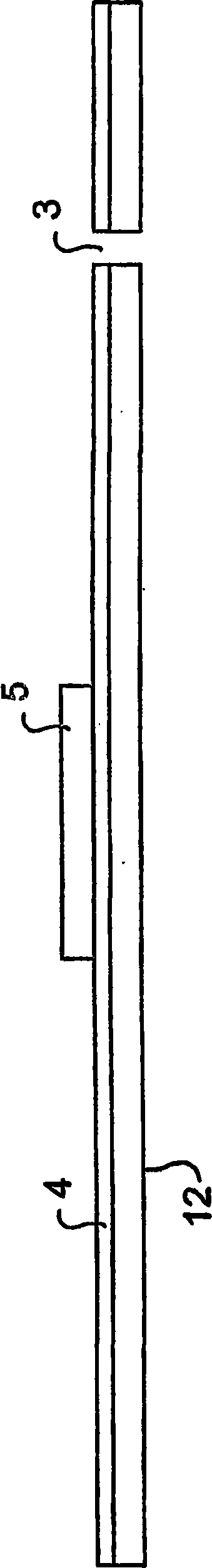
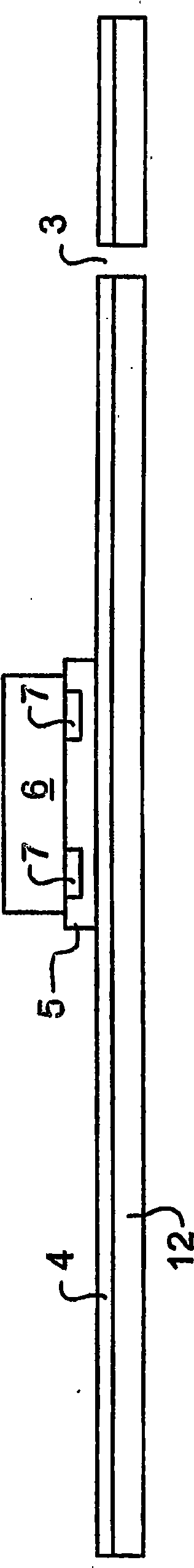
[0035] In the exemplary method, fabrication begins with a conductive layer 4, such as a metal layer. A suitable manufacturing material for the conductive layer 4 is a copper film (Cu). If the conductive film 4 selected for the process is very thin, or if it is mechanically not very robust for other reasons, it is advisable to support the conductive film 4 with the support layer 12 . This method can be used, for example, in such a way that the process proceeds from the production of the carrier layer 12 . The carrier layer 12 is, for example, a layer of an electrically conductive material, such as an aluminum layer, a steel layer, a copper layer, or a layer of an insulating material, such as a polymer layer. An unpatterned conductive layer 4 may be formed on the second surface of the support layer 4, for example, by some manufacturing methods well known in the circuit board industry. For example, a copper film may be laminated on the surface of the support layer 12, thereby p...


PUM


Abstract

This application discloses an electronic module and a method for manufacturing an electronic module, in which a component (6) is glued (5) to the surface of a conductive layer, from which conductive layer conductive patterns (14) are later formed. After gluing the component (6), an insulating-material layer (1), which surrounds the component (6) attached to the conductive layer, is formed on, or attached to the surface of the conductive layer. After the gluing of the component (6), feed-throughs are also made, through which electrical contacts can be made between the conductive layer and the contact zones (7) of the component. After this, conductive patterns (14) are made from the conductive layer, to the surface of which the component (6) is glued.

Description

[0001] This application is a divisional application of No. 200480009349.6 (PCT / FI2004 / 000195) patent application for invention submitted on March 31, 2004. 【Technical field】 [0002] The invention relates to an electronic module and to a method of manufacturing an electronic module. [0003] In particular, the invention relates to an electronic module comprising one or more components embedded in a mounting base. The electronic module may be a module such as a circuit board comprising several devices connected to each other by conductive members formed in the module. These devices may be passive devices, microcircuits, semiconductor devices or other similar devices. Usually the devices connected to the circuit board form a group of devices. Other important component groups are those that are usually packaged and connected to a circuit board. The electronic module referred to in the present invention certainly also includes other types of devices. 【Background technique】 ...

Claims


Application Information

Patent Timeline
Patent Type & Authority Applications(China)
IPC IPC(8): H01L25/00H01L23/48H01L21/60H05K1/18H05K3/46H01L23/538H01L25/065
CPCH01L2224/92144H01L2924/01082H01L2924/01002H01L2924/01327H01L2924/01029H01L24/19H01L2224/83192H01L2924/01027H01L2223/54473H01L2924/01087H01L25/0652H01L2924/014H01L2924/01013H01L23/544H01L2224/83191H01L2224/83855H01L2224/20H05K3/4611H01L2224/04105H01L2924/01005H01L2924/01033H01L2924/01006H01L2223/54426H01L2924/01078H01L2924/3025H05K1/188H01L23/5389H01L2224/32245H01L2224/83005H01L2224/83132H01L2924/07802H01L2924/12042H01L2924/3511H01L2924/00H05K1/18
Inventor R·托明恩P·帕姆
Owner IMBERATEK LLC
Why Eureka
Try Eureka