High power light emitting diode module package structure

A light-emitting diode and module packaging technology, used in semiconductor devices, electrical components, circuits, etc., can solve the problems of poor adhesion, inability to meet users, and expensive LED module manufacturing process.

Inactive Publication Date: 2009-09-30
BRIDGE SEMICON
View PDF0 Cites 16 Cited by
  • Summary
  • Abstract
  • Description
  • Claims
  • Application Information

AI Technical Summary

Problems solved by technology

[0009] Although the component pads of the above-mentioned heat dissipation substrate and the heat dissipation plate are the same or integrally formed metal, the circuit is directly grown on the matured insulating material 91, so there are reliability problems such as poor adhesion; in addition, In addition to the expensive m

Method used


Image

  • High power light emitting diode module package structure
  • High power light emitting diode module package structure
  • High power light emitting diode module package structure

Examples


Embodiment Construction

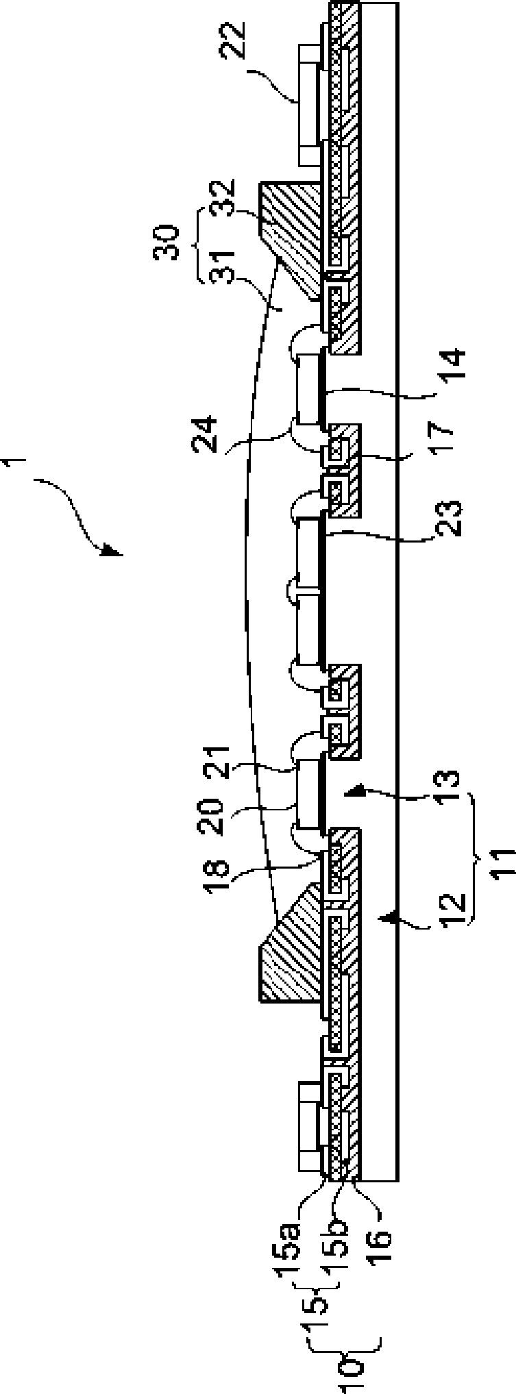
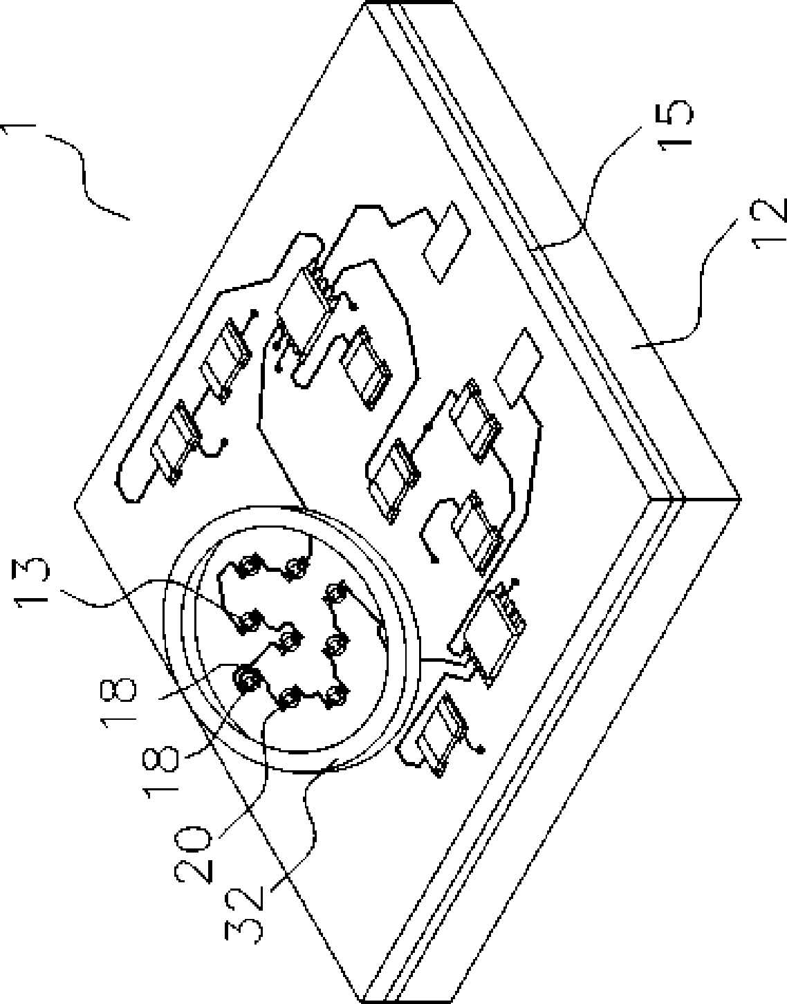
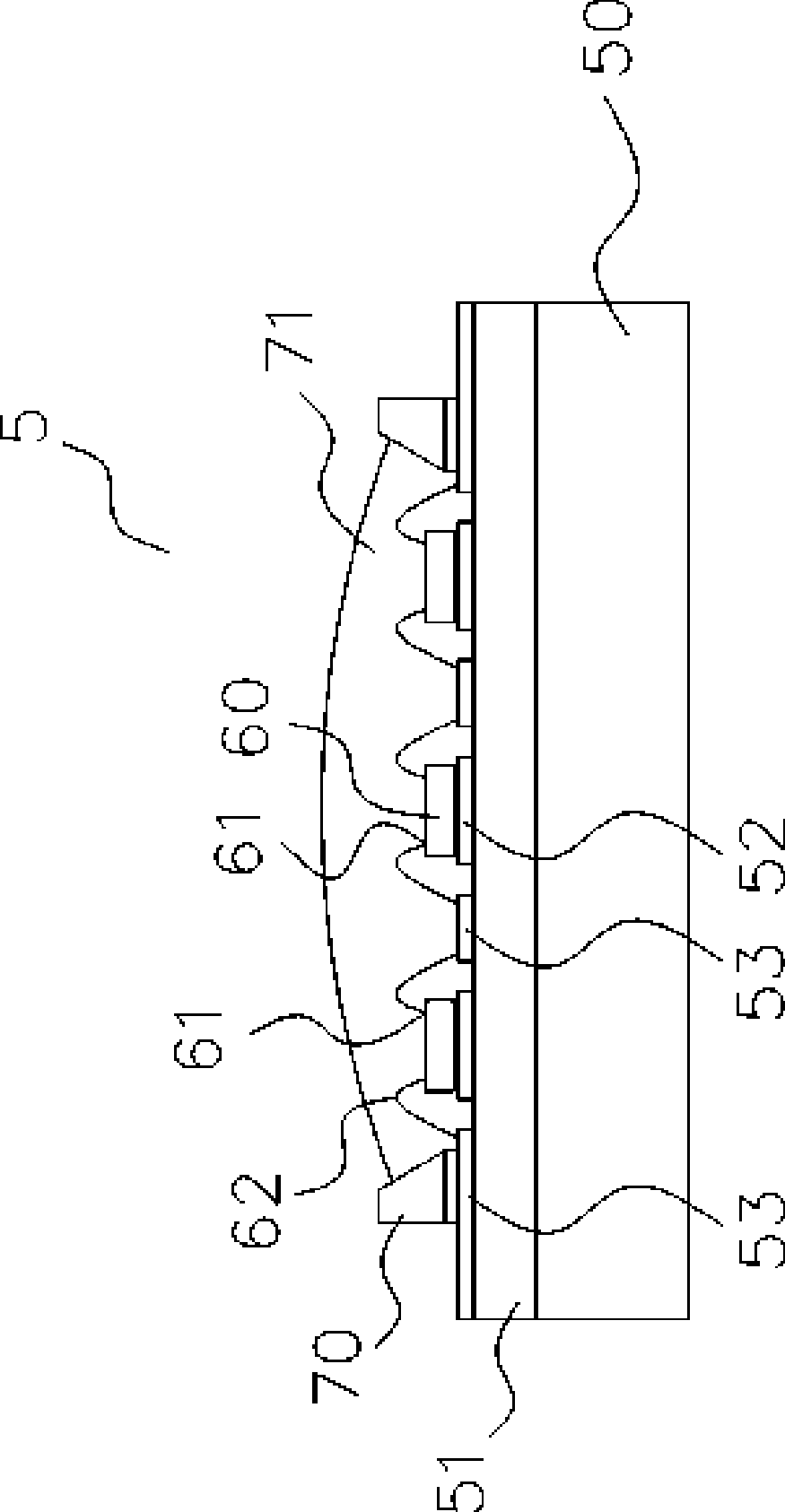
[0046] The invention relates to a high-power LED module packaging structure, which at least includes a substrate, a LED and an insulating casing.

[0047] The substrate includes a heat dissipation base and a multi-layer circuit. The heat dissipation base includes a base and at least one component joint post protruding from the base. The surface of the component joint post is smaller than the surface of the base, so that The component bonding post is directly bonded to the light-emitting diode, and the multi-layer circuit is pressed on the base with the raised component bonding post as the core and extends around, and an insulating layer is placed between the component bonding post. Bond without any gaps or other material. Wherein, the surface of the component joint post is smaller than the surface of the base; the multilayer circuit may include one or more layers of circuits, and the upper and lower circuits can be electrically connected by laser plating holes, mechanical plat...


PUM


Abstract

A high power light emitting diode module package structure at least comprises a substrate, a plurality of light emitting diodes and an insulated housing; wherein the substrate comprises a radiating base and multilayer line; the substrate is directly joined with the light emitting diode based on the assembly joining column raised on the radiating base, thereby effectively educing the heat source produced when running the light emitting diode; further, the multilayer line surrounding the assembly joining column can provide the winding for electrically connecting the assemblies in the module for strengthening the elasticity of the pattern design, thereby making a purpose of customized module, and having high reliability, high design elasticity, high thermal diffusivity and low cost.

Description

Technical field: [0001] The invention relates to a high-power light-emitting diode module package structure, in particular to a heat dissipation requirement for high-power chips and a modular light-emitting diode package structure. Background technique: [0002] With the popularity of optoelectronic products and the continuous improvement of the power of LED chips, the modularization of multi-chip LEDs has gradually become a new trend in electronic lighting. Therefore, as the substrate for the electrical connection of LED multi-chip modules, its winding ability and heat dissipation It has become one of the key factors for the smooth development of new products. [0003] The heat-dissipating aluminum substrate developed in the early stage has the problem of poor overall heat-dissipating effect due to the resin contained below the position of the light-emitting diode components. see image 3 As shown in FIG. 1 , it is a cross-sectional schematic diagram of a package structure...

Claims


Application Information

Patent Timeline
IPC IPC(8): H01L25/075H01L33/00
CPCH01L2924/12041H01L2224/48091H01L2224/73265H01L2224/48227H01L2924/00011H01L2224/48137H01L2924/00H01L2924/00014H01L2924/01005
Inventor 王家忠
Owner BRIDGE SEMICON
Why Eureka
Try Eureka