Polycrystalline packaging unit and manufacture method thereof

A manufacturing method and encapsulation colloid technology, which is applied in semiconductor/solid-state device manufacturing, electrical components, electric solid-state devices, etc., can solve problems such as little improvement in luminous efficiency, high cost, and complicated circuit layout, so as to reduce production costs , cost reduction, good luminous efficiency

Inactive Publication Date: 2009-10-07
XIAMEN LIGHT TREND OPTOELECTRONICS TECH
View PDF0 Cites 12 Cited by
  • Summary
  • Abstract
  • Description
  • Claims
  • Application Information

AI Technical Summary

Problems solved by technology

[0007] 2. The substrate (8) can only be set for one die (70), and the brightness is limited. When a high measurement is required, multiple units need to be installed, which requires a large space, complicated circuit layout, and poor heat dissipation. problems will happen
[0009] 3. Because it is to be used as a lighting source, but the heat generated is still high, so it must be installed with heat dissipation devices, such as heat dissipation fins, water cooling devices and other systems, so that it can be used with peace of mind. Therefore, it consumes a lot of money in lamp manufacturing and materials. more cost, more cost
[0011] 4. Although it is installed on the metal plate (80), because there is only one single grain (70), the luminous efficiency is still not much improved, and the brightness and lifespan will be deteriorated due to the influence of long-term high temperature environment. shortened question

Method used


Image

  • Polycrystalline packaging unit and manufacture method thereof
  • Polycrystalline packaging unit and manufacture method thereof
  • Polycrystalline packaging unit and manufacture method thereof

Examples


Embodiment Construction

[0051] Specific embodiments of the present invention are described below in conjunction with accompanying drawing:

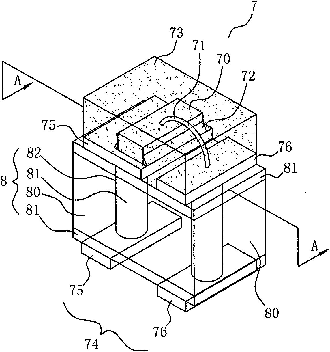
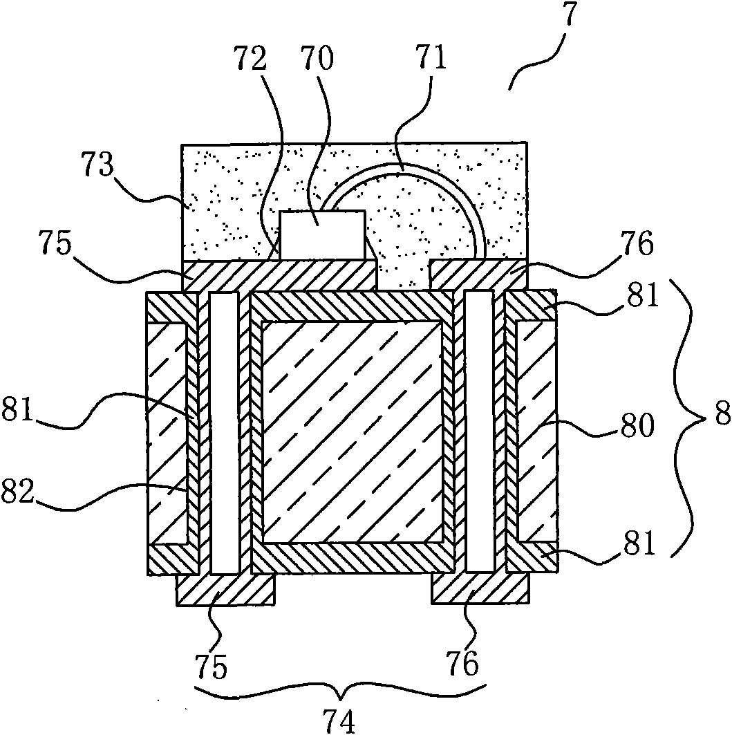
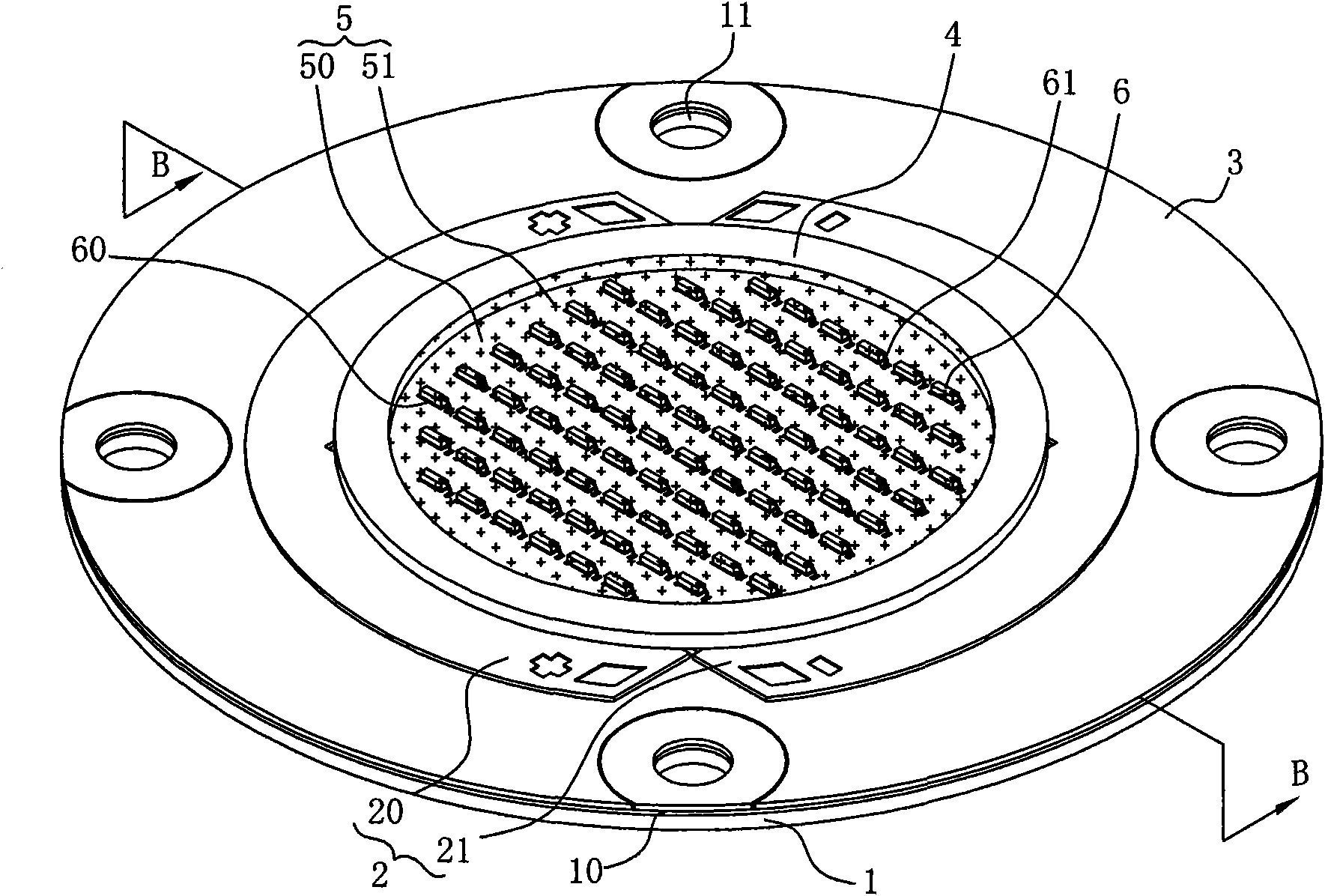
[0052] Such as image 3 Shown is a three-dimensional schematic diagram of the present invention, as Figure 4 shown as image 3 A schematic diagram of the B-B section.

[0053] The figure reveals that a polycrystalline packaging unit includes: a substrate 1 with high heat dissipation, made of metal, and in the shape of a thin plate, the substrate 1 is provided with an insulating layer 10 arranged on the surface of the substrate 1, a set On the top side of the insulating layer 10, a circuit layer 2 that can be connected to the power line; and a protective layer 3 that is provided on the top side of the circuit layer 2 and can be used to cover the circuit; at least one is provided on the surface of the protective layer 3 , which is smaller than the substrate 1 and has a hollow fixed frame 4; several LED crystal grains 6 which are arranged in the fixed frame 4 a...


PUM


Abstract

The invention discloses a polycrystalline packaging unit, comprising a substrate (1), at least one hollow fixed frame (4), a plurality of LED crystal grains (6) and a packaging colloid (5), wherein the substrate (1) has high heat radiation, is made of metals to be in a shape of thin plate, and is provided with an insulating layer (10) on the surface, a circuit layer (2) arranged on the top of the insulating layer (10) to be connected with a power cord, and a protective layer (3) which is arranged on the top of the circuit layer (2) to be used for covering circuits and has insulating performance; the fixed frame (4) is arranged on the surface of the protective layer (3) and is smaller than the substrate (1); the LED crystal grains (6) are arranged in the fixed frame (4) and is electrically connected with the circuit layer (2); and the packaging colloid (5) is arranged in the fixed frame (4), covers the LED crystals (6) and has light transmission. The polycrystalline packaging unit has the advantages of simple manufacture, favorable heat radiation and high brightness.

Description

technical field [0001] The invention relates to a polycrystalline packaging unit and a manufacturing method thereof. Background technique [0002] Conventional surface-mount device LED configurations, such as figure 1 , figure 2 As shown, it is known that it is a surface mount light-emitting diode (7) with high heat dissipation, which includes a substrate (8) with high heat dissipation and is located on the substrate (8), and the colloid (73 ), characterized in that the substrate (8) includes: a metal plate (80), the substrate (8) is used to carry the support of the colloid (73), and has a plurality of through holes (82); an insulating layer ( 81), coating a layer of insulating material on the surface of the metal plate (80) and the inner wall of the through hole (82), the thickness of the insulating layer (81) is smaller than the thickness of the metal plate (80); and a circuit layer (74 ), located on the surface of the insulating layer (81) and in the through hole (82)...

Claims


Application Information

Patent Timeline
Patent Type & Authority Applications(China)
IPC IPC(8): H01L25/00H01L25/075H01L23/36H01L23/488H01L23/31H01L21/50H01L21/60H01L21/56
CPCH01L24/97H01L2224/48091H01L2224/73265H01L2224/48227H01L2224/32225H01L2224/97
Inventor 黄一峰沈昌钧
Owner XIAMEN LIGHT TREND OPTOELECTRONICS TECH
Why Eureka
Try Eureka