Supercharge Your Innovation With Domain-Expert AI Agents!

Method for manufacturing electronic component supporting plate

A technology for electronic components and manufacturing methods, which is applied in the directions of electrical components, multilayer circuit manufacturing, and electrical connection formation of printed components, and can solve the problems of inability to replace multilayer circuit boards and low circuit density.

Inactive Publication Date: 2011-09-21
SUBTRON TECH
View PDF0 Cites 0 Cited by
  • Summary
  • Abstract
  • Description
  • Claims
  • Application Information

AI Technical Summary

Problems solved by technology

However, the known flexible circuit board has the disadvantage of low circuit density because it has only one layer of circuit, and cannot replace the multilayer circuit board.

Method used


Image

  • Method for manufacturing electronic component supporting plate
  • Method for manufacturing electronic component supporting plate
  • Method for manufacturing electronic component supporting plate

Examples


Embodiment Construction

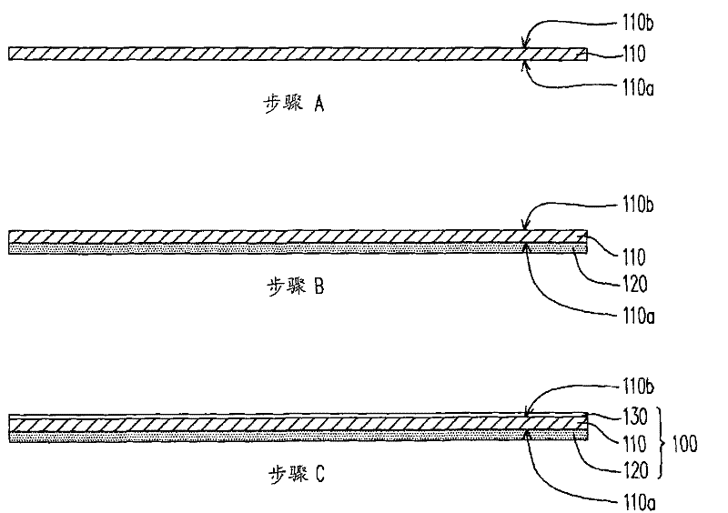
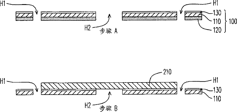
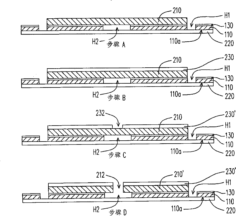
[0028] Figure 1A-1E It is a schematic diagram of steps of a method for manufacturing an electronic component carrier according to an embodiment of the present invention. It should be stated in advance that, Figure 1A-1E The manufacturing method of the electronic component carrier shown is only for illustration, so that those skilled in the art of the present invention can implement it, so the scope of the present invention is not limited to Figure 1A-1E The disclosed manufacturing method of the electronic component carrier also includes other embodiments not disclosed in the drawings. For this reason, the scope of the present invention should still be defined by the claims.

[0029] see Figure 1A , Figure 1A Steps A to C in the above are to fabricate the base material 100 . In detail, first, step A is performed to provide the first conductive layer 110 . The first conductive layer 110 may be a metal foil, such as copper foil, aluminum foil, or foil made of other sui...


PUM


Abstract

The invention discloses a method for manufacturing an electronic component supporting plate, which comprises the following steps: firstly, forming a plurality of first through holes and at least one second through hole on base material which comprises a first conducting layer; then, forming a second conducting layer which covers the second through hole on the base material; patterning the second conducting layer to form at least one opening communicated with the second through hole; and then, patterning the first conducting layer, thus the method for manufacturing the electronic component supporting plate can be used for manufacturing an electronic component supporting plate with multi-layer circuits.

Description

technical field [0001] The invention relates to a packaging process for electronic components, and in particular to a method for manufacturing an electronic component carrier. Background technique [0002] Nowadays, semiconductor technology is advanced, and many chips (chips) have a large number of transistor (transistor) elements arranged in high density. In order to use these chips, many chip carriers have been developed towards the characteristics of high line density and narrow line pitch (fine pitch). [0003] Today's chip carrier boards can be mainly divided into two types: one is a rigid circuit board, and the other is a flexible circuit board. In order to increase the circuit density and reduce the circuit pitch of the rigid circuit board, a multilayer circuit board (multilayer circuit board) with a multilayer circuit structure has been developed. The circuit structure of this kind of multilayer circuit board is mostly made by laminated method or laminated method (...

Claims


Application Information

Patent Timeline
Patent Type & Authority Patents(China)
IPC IPC(8): H05K3/40H01L21/48H05K3/46
Inventor 吴建男杨耿忠黄维乾
Owner SUBTRON TECH
Features
  • R&D
  • Intellectual Property
  • Life Sciences
  • Materials
  • Tech Scout
  • Unparalleled Data Quality
  • Higher Quality Content
  • 60% Fewer Hallucinations
Learn More