Resistance structure for improving silicon-on-insulator (SOI) circuit ESD protection network

A resistance structure and network technology, applied in circuits, electrical components, electrical solid devices, etc., can solve the problems of easy burnout of resistors, and achieve the effect of reducing room temperature resistance, overcoming easy burnout, and improving ESD resistance.

Active Publication Date: 2009-10-21
INST OF MICROELECTRONICS CHINESE ACAD OF SCI
View PDF0 Cites 4 Cited by
  • Summary
  • Abstract
  • Description
  • Claims
  • Application Information

AI Technical Summary

Problems solved by technology

[0006] In view of this, the present invention is aimed at the above-mentioned problem, provides a kind of resistance structure that improves the SOI circuit ESD protection network, to reduce the negative impact on circuit electrical performance; Current situation, to solve the problem that the resistance of the present invention is easy to burn

Method used


Image

  • Resistance structure for improving silicon-on-insulator (SOI) circuit ESD protection network
  • Resistance structure for improving silicon-on-insulator (SOI) circuit ESD protection network
  • Resistance structure for improving silicon-on-insulator (SOI) circuit ESD protection network

Examples


Embodiment Construction

[0026] In order to make the object, technical solution and advantages of the present invention clearer, the present invention will be described in further detail below in conjunction with specific embodiments and with reference to the accompanying drawings.

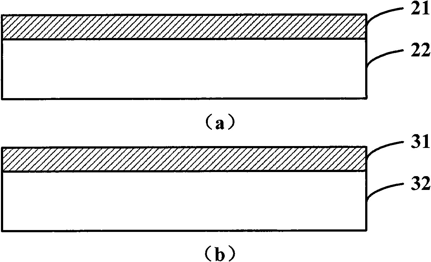
[0027] Such as figure 1 As shown, the present invention uses silicon 22 or silicides 21 and 31 on polysilicon 32 as a resistive and conductive thin film, which is a resistive structure for ESD protection network. The silicon 22 or polysilicon 32 can be any doped SOI silicon film or polysilicon film whose sheet resistance is more than 5 times larger than that of the corresponding silicides 21 and 31 . The silicides 21 and 31 refer to a compound formed by a physical-chemical reaction between metal and silicon, which has a conductivity between metal and semiconductor, mainly including titanium silicide, cobalt silicide or nickel silicide.

[0028] In this resistance structure, the silicide film plays the main role of conduc...


PUM


Abstract

The invention relates to the technical field of semiconductors and discloses a resistance structure for improving a silicon-on-insulator (SOI) circuit ESD protection network. By using the conductor characteristics of silicide, the structure solves the problem that a semiconductor current carrier conducting resistance structure enables resistance not to reduce the resistance value and the potential lifting capability of resistance but increase the resistance value and improve the potential lifting capability of the resistance in a large-scale ESD process at high temperature because of the characteristics of the resistance negative temperature generated by the intrinsic ionization effect. In addition, the resistance also has the stable resistance value characteristics after ESD, the problem of the impurity tempering effect generated in the ESD process of the semiconductor current carrier conducting resistance is solved, and the effect on electrical properties of a circuit is further reduced. By using the invention, on one hand, more stable ESD protecting capability can be obtained, on the other hand, the effect on the electrical properties of a circuit by the resistance for protecting the ESD can be reduced when more stable ESD protecting capability is obtained.

Description

technical field [0001] The invention relates to the technical field of semiconductors, in particular to a resistance structure for improving the ESD protection network of SOI circuits. Background technique [0002] With the development of the semiconductor industry, especially after entering the deep submicron scale, on the one hand, the breakdown voltage of the oxide layer will be greatly reduced; The anti-electrostatic discharge protection (ESD) capability of the drain end of the output tube also becomes very poor. In order to improve the ESD current discharge capability of the SOI circuit itself under the limited conduction capability of the SOI metal oxide semiconductor (MOS) structure, a resistor structure must be connected in series at the output end / bidirectional end of the SOI circuit, so that the output end / bidirectional end of the circuit When the reverse bias ESD voltage is applied to the diode, the voltage obtained on the output terminal / bidirectional terminal p...

Claims


Application Information

Patent Timeline
Patent Type & Authority Applications(China)
IPC IPC(8): H01L27/12H01L23/60
Inventor 曾传滨李晶海潮和李多力韩郑生
Owner INST OF MICROELECTRONICS CHINESE ACAD OF SCI
Why Eureka
Try Eureka