Liquid crystal display panel and manufacturing method thereof
A technology of liquid crystal display panels and manufacturing methods, applied in semiconductor/solid-state device manufacturing, optics, instruments, etc., can solve the problems of large non-display area, small signal attenuation, and large signal attenuation, and achieve small area and small attenuation Effect
- Summary
- Abstract
- Description
- Claims
- Application Information
AI Technical Summary
Problems solved by technology
Method used
Image

Examples
Embodiment Construction
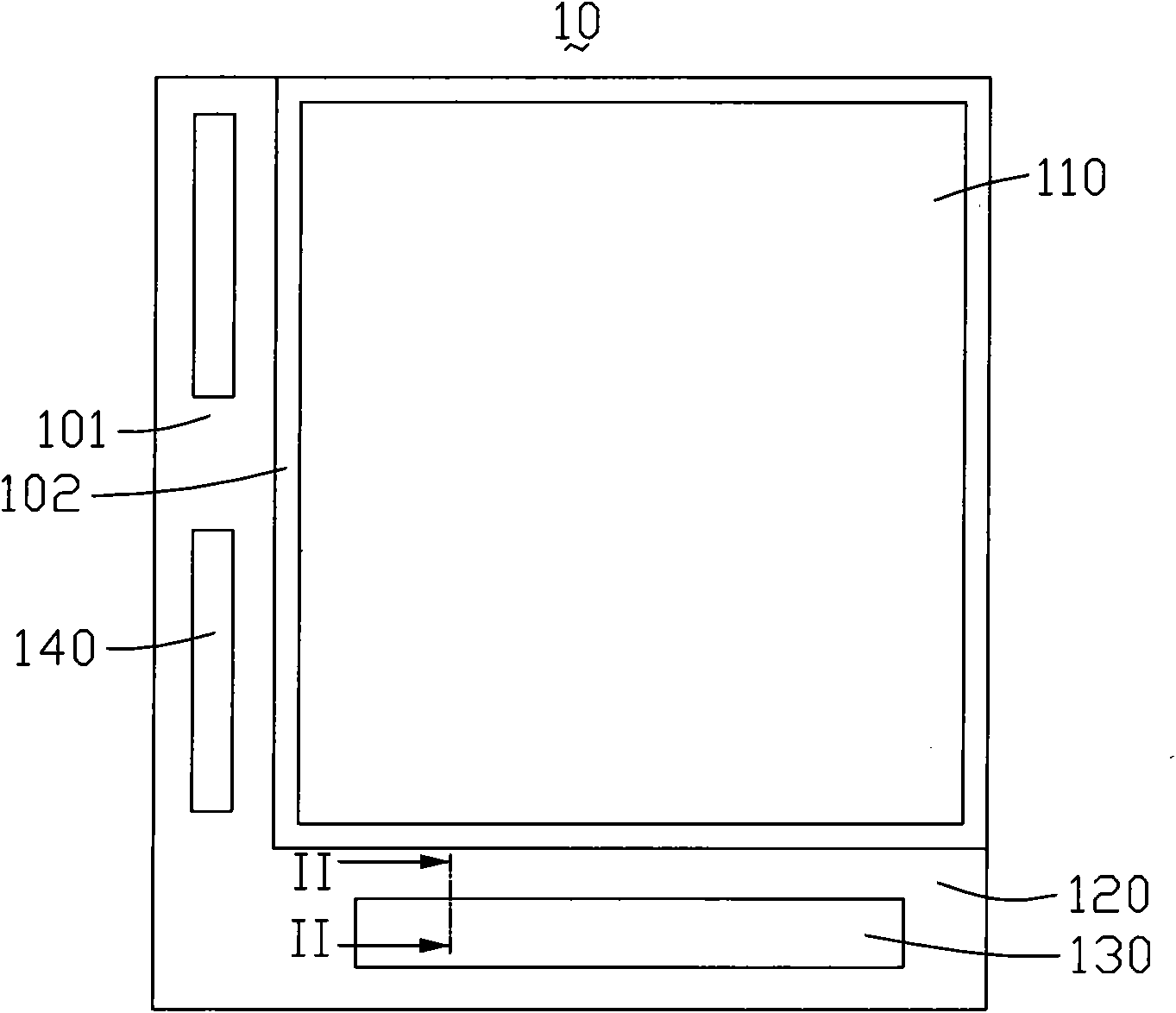
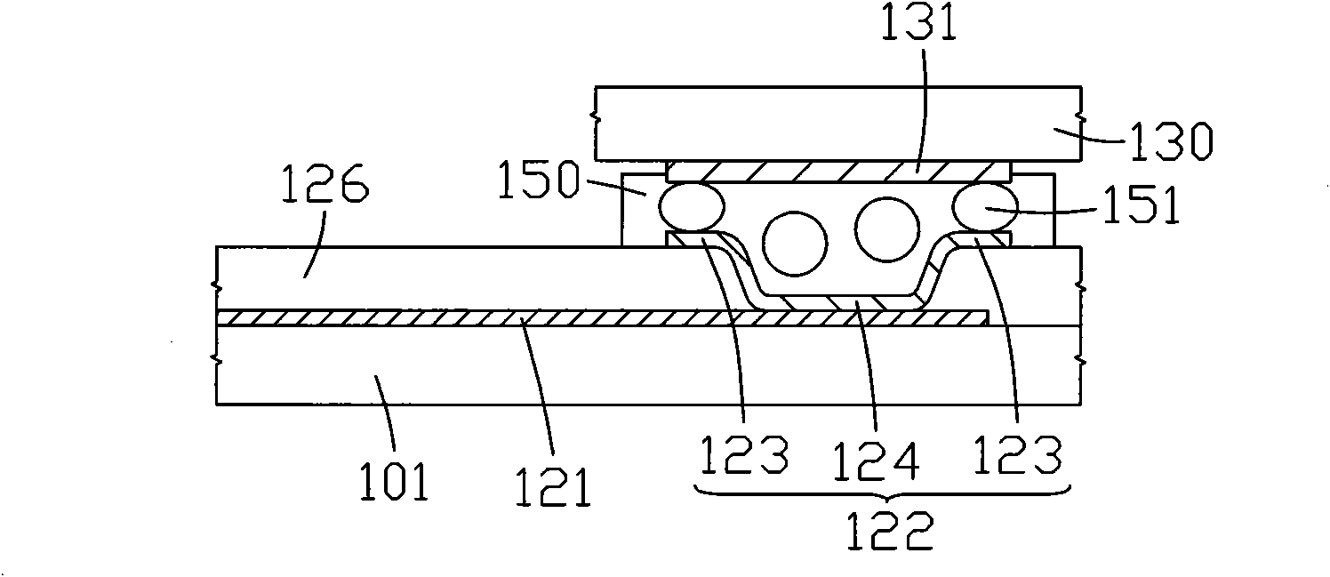
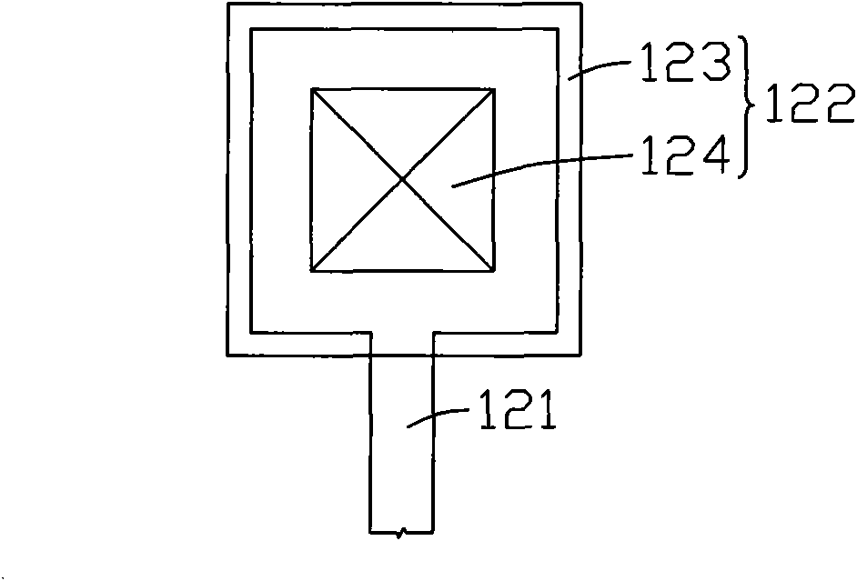
[0031] see Image 6 and Figure 7 , Image 6 is a schematic plan view of the first embodiment of the liquid crystal display panel of the present invention, Figure 7 Yes Image 6 The schematic cross-sectional view of the liquid crystal display panel along the VII-VII direction is shown. The liquid crystal display panel 30 includes a TFT substrate 301 and a color filter substrate 302 . The color filter substrate 302 is disposed opposite to the TFT substrate 301 and has an area smaller than that of the TFT substrate 301 . A portion of the TFT substrate 301 overlapping the color filter substrate 302 defines a display area 310 , and a portion of the TFT substrate 301 not overlapping the color filter substrate 320 defines a non-display area 320 . A liquid crystal layer 303 is disposed between the TFT substrate 301 and the color filter substrate 302 corresponding to the display area 310 .
[0032] The non-display area 320 includes a scan driver 330, two data drivers 340, a plu...
PUM
 Abstract
Description
Claims
Application Information
 - Generate Ideas
- Intellectual Property
- Life Sciences
- Materials
- Tech Scout
- Unparalleled Data Quality
- Higher Quality Content
- 60% Fewer Hallucinations
Browse by: Latest US Patents, China's latest patents, Technical Efficacy Thesaurus, Application Domain, Technology Topic, Popular Technical Reports.
© 2025 PatSnap. All rights reserved.Legal|Privacy policy|Modern Slavery Act Transparency Statement|Sitemap|About US| Contact US: help@patsnap.com