One-time programming memory and manufacturing method thereof
What is AI technical title?
AI technical title is built by PatSnap AI team. It summarizes the technical point description of the patent document.
A manufacturing method and memory technology, applied in the field of microelectronics, can solve the problems of read crosstalk, 1R structure integration limitation, increase design complexity and cost, etc., and achieve the effect of eliminating influence, facilitating integration and use, and suppressing read crosstalk.
Inactive Publication Date: 2009-11-11
INST OF MICROELECTRONICS CHINESE ACAD OF SCI
View PDF0 Cites 9 Cited by
Summary
Abstract
Description
Claims
Application Information
AI Technical Summary
This helps you quickly interpret patents by identifying the three key elements:
Problems solved by technology
Method used
Benefits of technology
Problems solved by technology
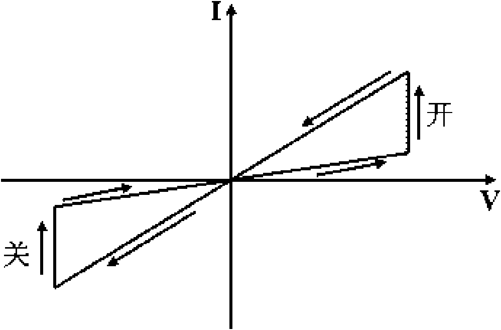
From this it can be seen that the use of figure 1 The integrated solution based on the 1R structure of the electrical characteristics shown has a serious problem of read crosstalk. If the read crosstalk is avoided through carefully designed peripheral circuits, the complexity and cost of the design will inevitably increase, which will make the figure 1 The integration of 1R structures with symmetric transition properties shown is limited by
Method used
Image
Click on the blue label to locate the original text in one second.
Reading with bidirectional positioning of images and text.
Examples
Embodiment 1
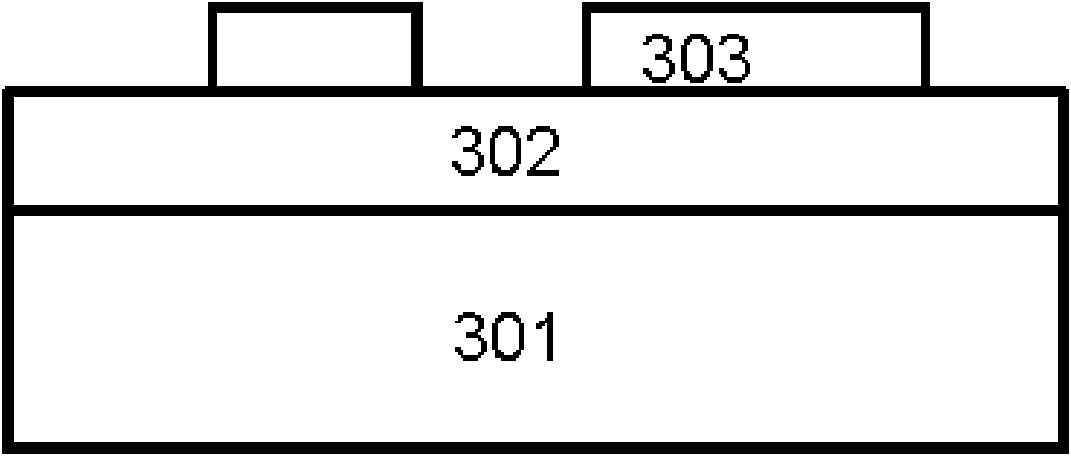
[0033] see image 3 , the embodiment of the present invention proposes a one-time programming memory device that can be integrated with a cross-array structure and has a rectification function. The one-time programming memory includes:
[0034] lower electrode 301;
[0035] upper electrode 303; and
[0036] The functional layer film 302 is located between the upper electrode 303 and the lower electrode 301 .
[0037] The upper electrode 303 and the lower electrode 301 are made of Pt, Ag, Pd, W, Ti, Al, Cu, TiN, ITO, IZO, YBCO, LaAlO 3 , SrRuO 3 and any material in polycrystalline Si. In this embodiment, the upper electrode 303 uses Pt, and the lower electrode 301 uses n + Si.
[0038] The functional layer film 302 adopts NiO, TiO x , CuO x , ZrO x , TaO x , AlO x , CoO, HfO x 、MoO x , ZnO, PCMO, LCMO, SrTiO 3 , BaTiO 3 , SrZrO and any one of amorphous silicon materials. Functional layer film 302 adopts ZrO in the present embodiment2 . In addition, the function...
Embodiment 2
[0045] see Figure 5 , the embodiment of the present invention also provides a method for manufacturing a one-time programming memory, including the following steps:
[0046] Step 501: forming a substrate as a lower electrode;
[0050] Step 503: Carry out photolithography and deposit conductive material on the functional la...
PUM
Abstract
The invention relates to a one-time programming memory and a manufacturing method thereof, belonging to the technical field of microelectronics. The one-time programming memory comprises a lower electrode, an upper electrode and a functional layer film positioned between the upper electrode and the lower electrode; the contact between the upper electrode and the functional layer film or between the lower electrode and the functional layer film forms rectification characteristics. The manufacturing method of the one-time programming memory comprises the steps: forming a substrate as the lower electrode; forming the functional layer film on the substrate; photoetching on the functional layer film and depositing conducting material to form the upper electrode after peeling-off; forming rectification characteristics in virtue of the contact between the upper electrode and the functional layer film or between the lower electrode and the functional layer film. The invention lowers manufacturing cost of the memory and is advantageous for integration and usage of the memory; memory devices can be integrated in a structure of cross array, thus enhancing density of the memory; the memory itself has the effect of rectification and no need of additional rectifying devices, thereby eliminating influence on the memory by the additional rectifying devices and prohibiting read crosstalk.
Description
technical field [0001] The invention relates to the technical field of microelectronics, in particular to a one-time programming memory and a manufacturing method thereof. Background technique [0002] Memory plays a very important role in the field of microelectronics technology. Memory can generally be divided into volatile and non-volatile memory. Volatile memory means that the information in the memory must be maintained when the power is turned on, and the stored information is lost when the power is turned off; instead of volatile memory, its main feature is that it can maintain the stored information for a long time without power on , it not only has the characteristics of ROM, but also has high access speed. With the demand for large-capacity and low-power storage in multimedia applications and mobile communications, the market share of non-volatile memory in semiconductor devices is becoming larger and larger, and it is also becoming a very important type of memor...
Claims
Application Information
Patent Timeline
Application Date:The date an application was filed.
Publication Date:The date a patent or application was officially published.
First Publication Date:The earliest publication date of a patent with the same application number.
Issue Date:Publication date of the patent grant document.
PCT Entry Date:The Entry date of PCT National Phase.
Estimated Expiry Date:The statutory expiry date of a patent right according to the Patent Law, and it is the longest term of protection that the patent right can achieve without the termination of the patent right due to other reasons(Term extension factor has been taken into account ).
Invalid Date:Actual expiry date is based on effective date or publication date of legal transaction data of invalid patent.

