Semiconductor element mounting structure and semiconductor element mounting method

A semiconductor and structure technology, which is applied in the fields of semiconductor/solid-state device parts, semiconductor devices, and semiconductor/solid-state device manufacturing, etc., can solve the problems of complicated manufacturing process and difficulty in configuring reinforcement members 711, etc., to reduce the area and reduce the thermal expansion difference. The effect of poor thermal shrinkage and prevention of internal breakage

Inactive Publication Date: 2009-11-11
PANASONIC CORP
View PDF3 Cites 12 Cited by
  • Summary
  • Abstract
  • Description
  • Claims
  • Application Information

AI Technical Summary

Problems solved by technology

[0013] In addition, in the semiconductor device mounting structure 701 of Patent Document 2, two kinds of resins are used for stress relief, so the manufacturing process becomes complicated.
Furthermore, there is also a problem that it is difficult to arrange the reinforcing member 711 for the thinned semiconductor element 2.

Method used


Image

  • Semiconductor element mounting structure and semiconductor element mounting method
  • Semiconductor element mounting structure and semiconductor element mounting method
  • Semiconductor element mounting structure and semiconductor element mounting method

Examples


no. 1 approach

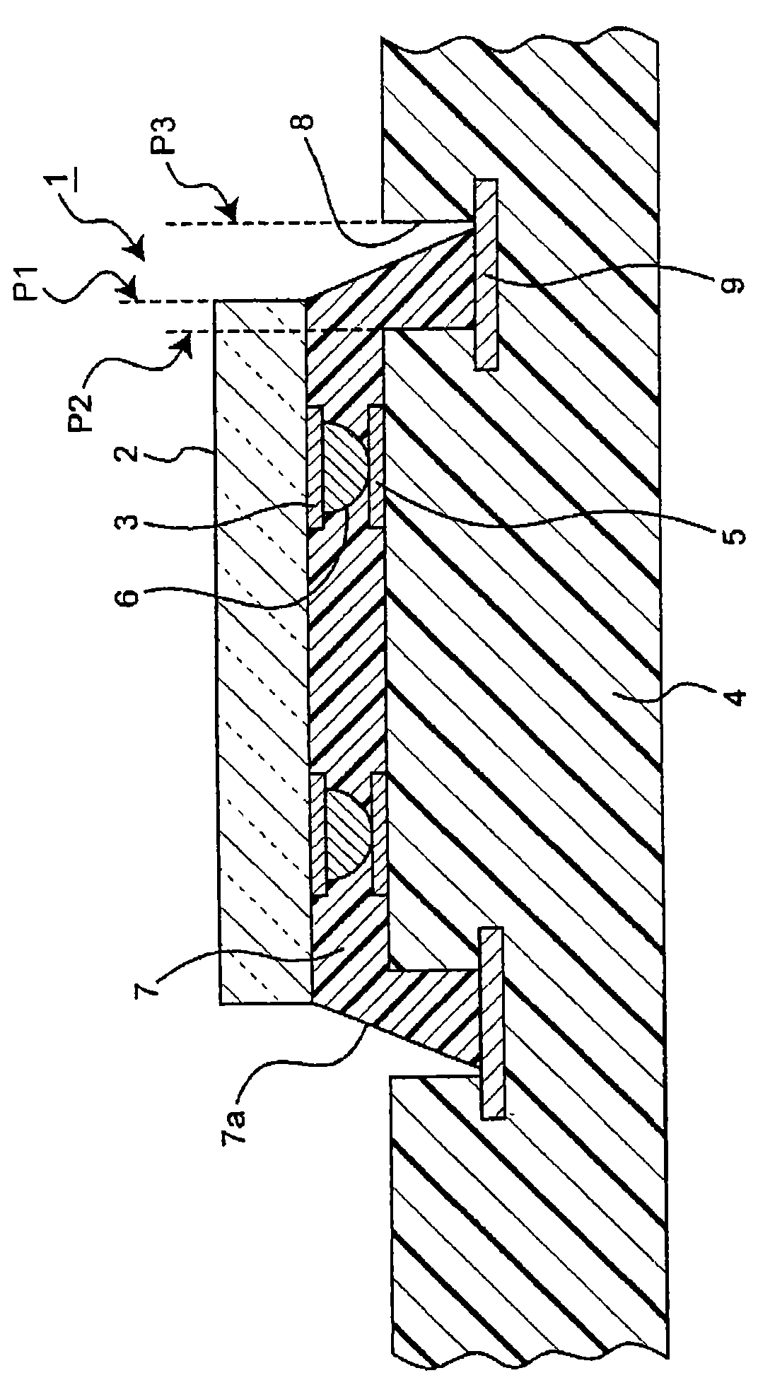
[0057] figure 1 A schematic cross-sectional view of a semiconductor chip mounting structure 1 as an example of the semiconductor element mounting structure according to the first embodiment of the present invention is shown in .

[0058] like figure 1 As shown, in the semiconductor chip mounting structure 1 of the first embodiment, a sheet-shaped underfill 7 as an example of a resin for sealing and bonding is disposed on a substrate 4, and a semiconductor chip 2 is mounted through the underfill 7. . A plurality of pads 3 as an example of element electrodes are formed on the lower surface side in the figure of the semiconductor chip 2, that is, on the circuit formation surface, and are formed on the upper surface side of the substrate 4 in a manner corresponding to the formation positions of these pads 3. That is, a plurality of substrate electrodes 5 are formed on the circuit formation surface (electrode formation surface), and each pad 3 and each substrate electrode 5 are...

no. 2 approach

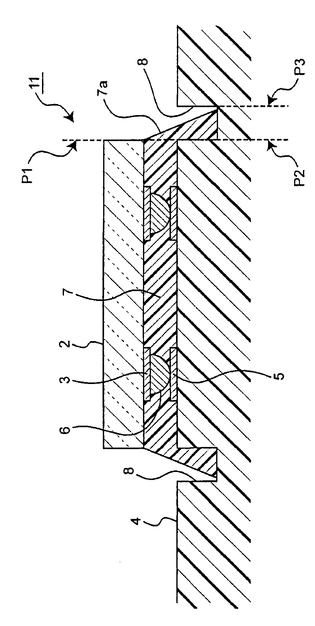
[0079] In addition, this invention is not limited to the said embodiment, It can implement in other various forms. E.g, Image 6 A schematic cross-sectional view of a semiconductor chip mounting structure 31 as an example of a semiconductor element mounting structure according to the second embodiment of the present invention is shown in . In addition, in Image 6 In the semiconductor chip mounting structure 31, members having the same configuration as those of the mounting structure 1 of the first embodiment are denoted by the same reference numerals, and description thereof will be omitted.

[0080] like Image 6 As shown, the semiconductor chip mounting structure 31 of the second embodiment has a different structure from the semiconductor chip mounting structure 1 of the above-mentioned first embodiment in that the inner bottom 38a of the recess 38 is formed as an inclined surface. . Hereinafter, this different structure will be mainly described.

[0081] like Image ...

no. 3 approach

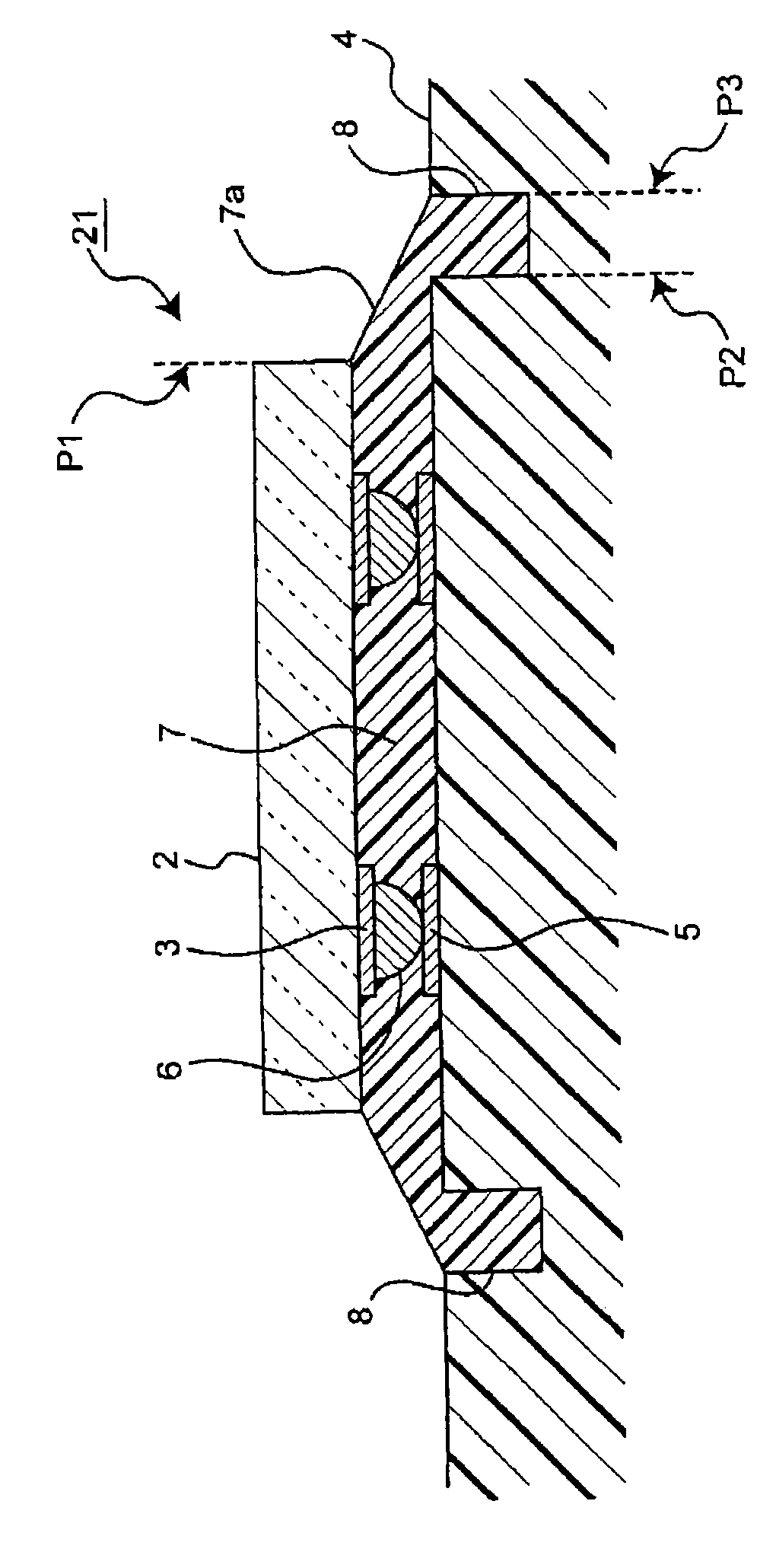
[0091] under, Figure 10 A schematic cross-sectional view of a semiconductor chip mounting structure 71 according to a third embodiment of the present invention is shown in . like Figure 10 As shown, the semiconductor chip mounting structure 71 of the third embodiment has the same Image 6 The mounting structure 31 of the above-mentioned second embodiment shown has the same arrangement structure of the recesses 38, but the fact that the protruding portion 79 is formed in the vicinity of the substantially center of the mounting area of ​​the substrate 4 compared with other surfaces is the same as Image 6 structure is different.

[0092] like Figure 10 As shown, by forming the raised portion 79 approximately in the vicinity of the center of the mounting area, a gradient is formed from the top of the raised portion 79 to the deepest portion of the recessed portion 38 via the sloped inner bottom 38a in the recessed portion 38 . Such gradients may be formed radially from, fo...


PUM


Abstract

On a substrate surface at a position facing an outer circumference end portion of a semiconductor element, a recessed section wherein a sealing adhesive resin is partially arranged is formed. Thus, while suppressing expansion of an arrangement region of a fillet portion (a portion spreading toward bottom) of the sealing adhesive resin, the inclination angle is increased. A stress load generated at the periphery of the semiconductor element due to thermal expansion differences and thermal shrinkage differences between members due to heating process and cooling process for mounting is reduced, and internal breakage of a semiconductor element mounting structure is eliminated.

Description

technical field [0001] The present invention relates to a mounting structure of a semiconductor element and a mounting method of the semiconductor element, wherein an element electrode of the semiconductor element is connected to a substrate electrode of a substrate through a protruding electrode, and a sealing adhesive is disposed between the semiconductor element and the substrate. A resin is used to mount the above-mentioned semiconductor element on the above-mentioned substrate. Background technique [0002] As an electronic device, when using a bare chip (bare chip) package that can greatly reduce the mounting area compared with conventional semiconductor packages, the circuit formation surface of the semiconductor chip (semiconductor element) and the circuit formation surface of the substrate are opposed to each other. Face-down mounting, in which conduction is obtained by overlapping bumps (protruding electrodes) made of metal such as gold, is compared to the circuit-...

Claims


Application Information

Patent Timeline
Patent Type & Authority Applications(China)
IPC IPC(8): H01L21/60H01L23/12
CPCH01L2224/75252H01L24/83H01L21/563H01L24/29H01L2224/32225H01L2224/83101H01L2224/83385H01L2224/27334H01L2224/16H01L2224/83194H01L2224/32057H01L2224/81191H01L2224/83051H01L2224/16225H01L2924/01004H01L23/49833H01L2924/01078H01L2224/27013H01L2924/01006H01L2224/73203H01L24/16H01L23/3185H01L2924/01079H01L2924/1579H01L2224/83192H01L24/13H01L2924/01005H01L2924/01082H01L2224/73204H01L2224/2919H01L2924/01013H01L2924/014H01L2924/15787H01L2924/01029H01L2924/30105H01L2224/838H01L23/13H01L24/32H01L2924/01019H01L2924/01033H01L2924/0665H01L2224/75315H01L2224/26175H01L24/75H01L2224/0554H01L2224/05568H01L2224/05573H01L2224/05624H01L2224/05644H01L2224/05655H01L2224/75316H01L2924/00014H01L2924/00H01L2924/00012H01L2924/3512H01L2224/05599H01L2224/0555H01L2224/0556
Inventor 户村善广光明寺大道
Owner PANASONIC CORP
Why Eureka
Try Eureka