
Positive photoresist, insulation layer and organic light emitting diode

A technology of light emitting diode and positive photoresist, applied in the field of organic light emitting diode components, can solve the problems of substrate residue, high voltage, pattern shedding, etc., and achieve the effects of improving contrast, low dielectric constant, and preventing light leakage.

Inactive Publication Date: 2009-11-18
KOLON IND INC
View PDF0 Cites 3 Cited by
  • Summary
  • Abstract
  • Description
  • Claims
  • Application Information

AI Technical Summary

Problems solved by technology

This is a higher voltage than if the pixel continued to emit light through the frame, resulting in less reliable long-term results
Second, significant voltage drop across the device due to the long and narrow shape of the electrodes and the high instantaneous current that induce high resistance
Through such a negative photoresist, for the interior of the coating film, the curing reaction moves from the surface to the bottom, and insufficient curing is prone to occur. The electrodes formed after forming the light-shielding cured film are prone to short circuit or curing. Adhesion between the film and the substrate is insufficient, and there are problems such as peeling off and chipping of the pattern after development
In addition, through traditional negative photolithography, the non-exposed parts formed by the radiation-resistant resin composition are prone to pollution problems such as residues on the substrate

Method used

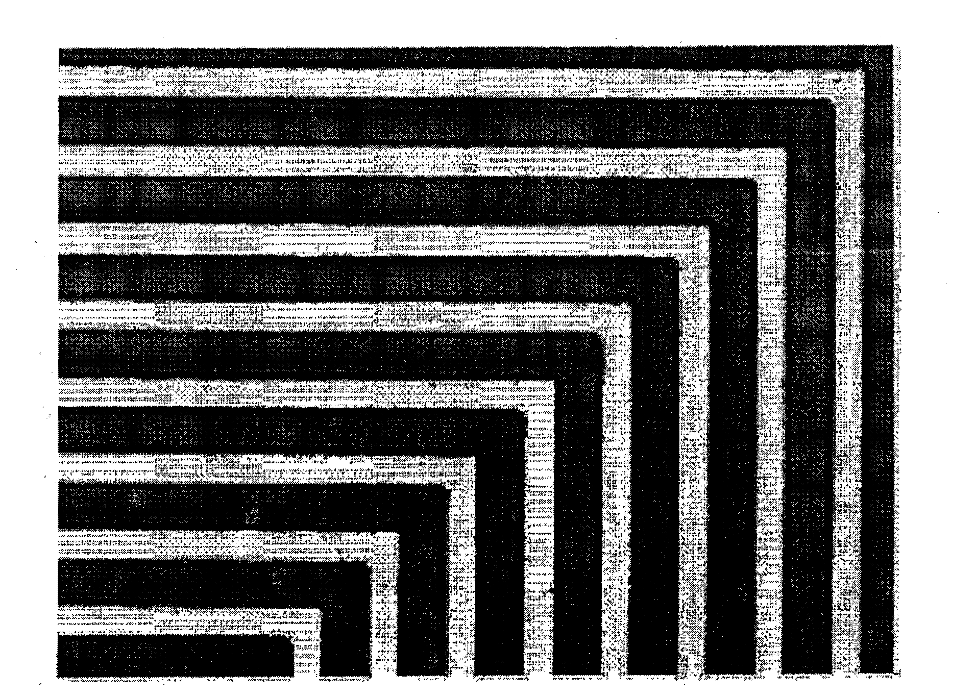
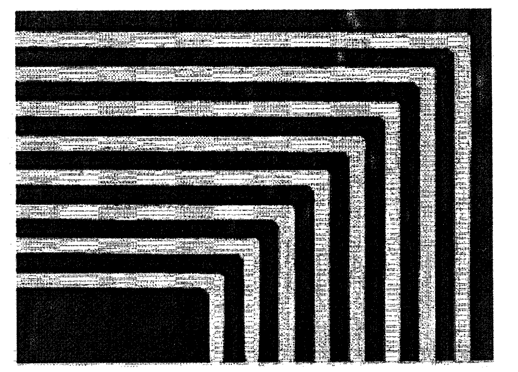
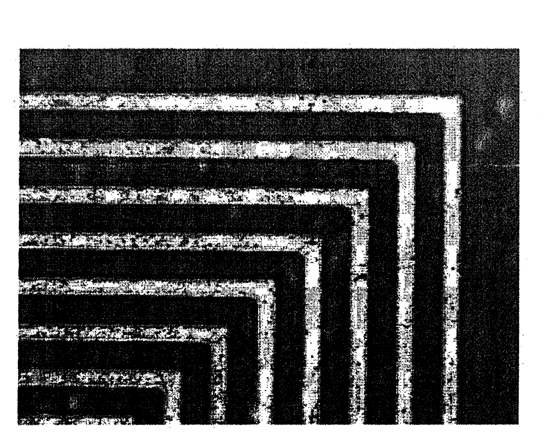

Image

  • Positive photoresist, insulation layer and organic light emitting diode
  • Positive photoresist, insulation layer and organic light emitting diode
  • Positive photoresist, insulation layer and organic light emitting diode

Examples


Embodiment 1

[0086] In order to prepare black pigment paste using pigment mixing components, 10 parts by weight of red pigment particles (C.I.PIGMENT RED 254), 4 parts by weight of blue pigment particles (C.I.PIGMENTBLUE 15:3) were mixed with propylene glycol monoethyl ether acetate as solvent , 1 part by weight of yellow pigment particles (C.I.PIGMENT yellow 139), 4 parts by weight of pigment dispersant (polyester resin, with a weight average molecular weight of 25,000), 1 part by weight of binder resin (polyacrylate resin, with a weight average molecular weight of 10,000) into a mixer for blending. The size of the dispersed pigment is 100nm or less. Here, the solvent was used in an amount of 80 parts by weight.

[0087] In the above-mentioned black pigment paste, add 15 parts by weight of novolac resins (cresol novolac resin, m-cresol and p-cresol are 4: 6 by weight, and the weight average molecular weight is 8,000 cresol novolak resin and The cresol novolac resin with a weight average...

Embodiment 2

[0105] According to the same composition and method as in Example 1 above, a positive-type photoresist was prepared, except that propylene glycol monoethyl ether acetate was used as a solvent, and 10 parts by weight of red pigment particles (C.I.PIGMENT RED 254), 4 parts by weight 1 part by weight of blue pigment particles (C.I.PIGMENT BLUE 15:3), 1 part by weight of yellow pigment particles (C.I.PIGMENT yellow139), 4 parts by weight of pigment dispersant (polyacrylate resin, weight average molecular weight 20,000), 1 part by weight of adhesive An agent resin (polyacrylate resin, weight average molecular weight: 10,000) was placed in a mixer and blended. The size of the dispersed pigment is 100nm or less. Here, the solvent was used in an amount of 80 parts by weight.

[0106] In the same manner as in Example 1, an insulating layer was formed using the fabricated positive-type photoresist and analyzed.

[0107] The analysis results are shown in Table 1.

Embodiment 3

[0109] According to the same composition and method as in Example 1 above, a positive-type photoresist was prepared, except that propylene glycol monoethyl ether acetate was used as a solvent, and 10 parts by weight of red pigment particles (C.I.PIGMENT RED 254), 4 parts by weight 1 part by weight of blue pigment particles (C.I.PIGMENT BLUE 15:3), 1 part by weight of yellow pigment particles (C.I.PIGMENT yellow139), 4 parts by weight of pigment dispersant (polyester resin, weight average molecular weight 25,000), 1 part by weight of binder Resin (polyacrylate resin, weight average molecular weight: 7,500) was placed in a mixer and blended. The size of the dispersed pigment is 100nm or less. Here, the solvent was used in an amount of 80 parts by weight.

[0110] In the same manner as in Example 1, an insulating layer was formed using the fabricated positive-type photoresist and analyzed.

[0111] The analysis results are shown in Table 1.


PUM

PropertyMeasurementUnit
thicknessaaaaaaaaaa
thicknessaaaaaaaaaa
thicknessaaaaaaaaaa

Abstract

The present invention provides a positive photoresist containing alkali-soluble resin, diazonium optical activity sensing compound and colorant, and no residue substances are generated when patterns are generated by using a black pigment paste capable of improving developing property of the patterns and the insulation resistance, and the positive photoresist has a low dielectric constant; the present invention also provides an insulation layer which has an optical activity blocking property, therefore, light leakage between adjacent pixels can be prevented, a contrast ratio is improved, andfinally a display with a high-definition picture quality can be provided.

Description

technical field [0001] The invention relates to a positive photoresist, the positive photoresist passes through an insulating layer formed by photolithography, and an organic light-emitting diode component with the insulating layer. Background technique [0002] At present, the simplest organic electroluminescent device includes: a positive electrode for injecting holes, a negative electrode for injecting electrons, and an organic medium interposed between the above two electrodes and used to support the recombination of charges. Such devices are often called organic light emitting diodes or OLEDs. For example, in order to form effective pixels in TVs, computer monitors, mobile phone display screens, or digital camera display screens, each OLED component can be formed by arranging pixels in a matrix. These pixels can produce a monochrome display device that emits a single color, or a red-green-blue (RGB) device that emits multiple colors. Organic light emitting diode compo...

Claims


Application Information

Patent Timeline
Patent Type & Authority Applications(China)
IPC IPC(8): G03F7/039G03F7/016H01L27/32
CPCG03F7/008G03F7/022G03F7/0233G03F7/032G03F7/0387G03F7/11
Inventor 朴世炯李炳逸金炳基
Owner KOLON IND INC
Learn More