Method for forming semiconductor interconnected structure

An interconnection structure and semiconductor technology, applied in semiconductor/solid-state device manufacturing, electrical components, circuits, etc., can solve problems such as electromigration, increased delay of semiconductor devices, and reduced clock frequency

Active Publication Date: 2009-11-25
SEMICONDUCTOR MANUFACTURING INTERNATIONAL (BEIJING) CORP
View PDF1 Cites 15 Cited by
  • Summary
  • Abstract
  • Description
  • Claims
  • Application Information

AI Technical Summary

Problems solved by technology

Since the etching gas used for plasma etching dielectric materials contains oxygen, an oxidizing atmosphere is formed. When the inner metal line is exposed to this oxidizing atmosphere, the metal line will partially form metal oxide, which will cause elec

Method used


Image

  • Method for forming semiconductor interconnected structure
  • Method for forming semiconductor interconnected structure
  • Method for forming semiconductor interconnected structure

Examples


Embodiment Construction

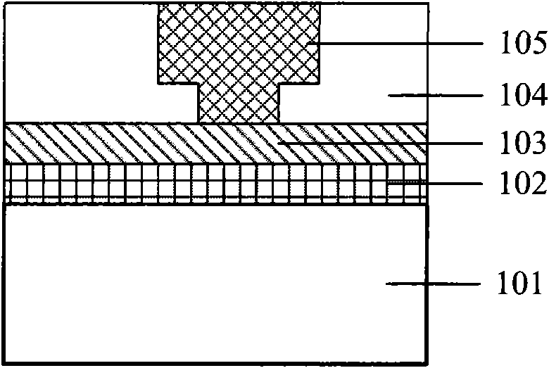
[0023] In this embodiment, by reducing the oxidized inner metal layer in the semiconductor metal interconnection structure, the acidic atmosphere in the subsequent process steps is prevented from corroding the inner metal layer, thereby improving the reliability of the manufactured semiconductor device, reducing delay and increasing Clock frequency.

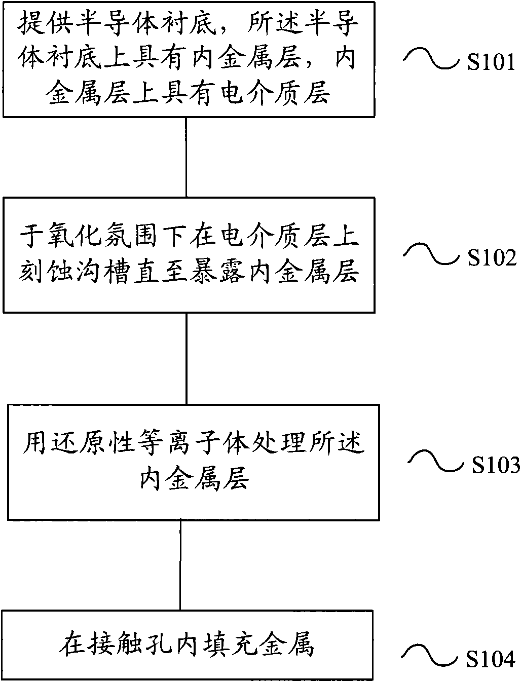
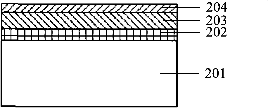
[0024] To this end, the present embodiment provides a method for forming a semiconductor interconnection structure, comprising the steps of: providing a semiconductor substrate, having an inner metal layer on the semiconductor substrate, and a dielectric layer on the inner metal layer; Etching a through hole until the inner metal layer is exposed; treating the inner metal layer with reducing plasma; filling the through hole with conductive material. Optionally, the reducing plasma is plasma containing hydrogen. Optionally, the process conditions for the hydrogen-containing plasma to treat the inner metal layer are hydrogen flow ...


PUM

PropertyMeasurementUnit
Etching poweraaaaaaaaaa

Abstract

The invention provides a method for forming a semiconductor interconnected structure, which comprises the following steps: providing a semiconductor substrate, wherein the semiconductor substrate is provided with an inner metal layer which is provided with a dielectric layer; etching a through hole on the dielectric layer until the inner metal layer is exposed in the atmosphere of oxidation; processing the inner metal layer by a reduction plasma; and filling a conducting material in the through hole. By performing the in-situ reduction of the oxidized inner metal layer in the semiconductor metal interconnected structure, the method prevents the acid atmosphere of the subsequent process procedures from corroding the inner metal layer, improves the reliability of the manufactured semiconductor devices, reduces the time delay and improves the clock frequency.

Description

technical field [0001] The invention relates to a semiconductor manufacturing process, in particular to a method for forming a semiconductor interconnection structure. Background technique [0002] A metal interconnect structure is a common structure included in semiconductor devices. This structure as figure 1 As shown, the surface of the semiconductor substrate 101 is covered with a dielectric layer 102, and the surface of the dielectric layer 102 forms an inner metal layer 103 with a pattern shape, and the dielectric layer 102 and the inner metal layer 103 are covered with an interlayer dielectric layer 104, and the interlayer dielectric layer 104 A groove for accommodating the outer metal layer 105 is opened thereon. [0003] The traditional semiconductor process mainly uses aluminum as the metal interconnect material, which has been limited in signal delay. Integrating the copper process into the integrated circuit manufacturing process can improve the integration le...

Claims


Application Information

Patent Timeline
IPC IPC(8): H01L21/768
Inventor 周鸣尹晓明
Owner SEMICONDUCTOR MANUFACTURING INTERNATIONAL (BEIJING) CORP
Why Eureka
Try Eureka