LED packaging method for high-power LED lighting fixtures
A technology of LED lighting and LED packaging, which is applied in the direction of lighting devices, cooling/heating devices of lighting devices, components of lighting devices, etc. Reduce the service life of LED light sources and other issues, and achieve the effect of easy modularization and modularization, broadening the scope of application, and novel, reasonable and compact structure
- Summary
- Abstract
- Description
- Claims
- Application Information
AI Technical Summary
Problems solved by technology
Method used
Image

Examples
Embodiment 1
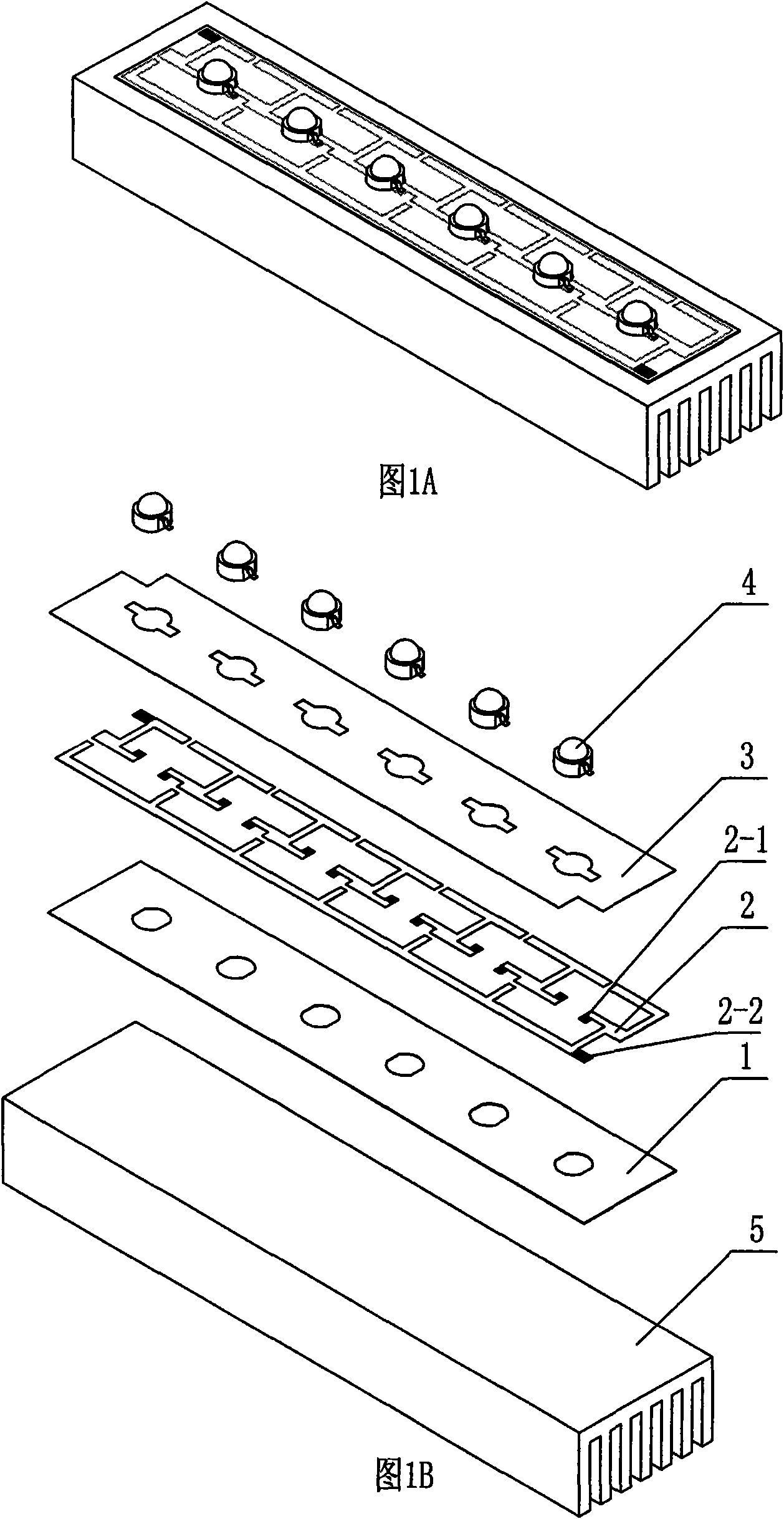
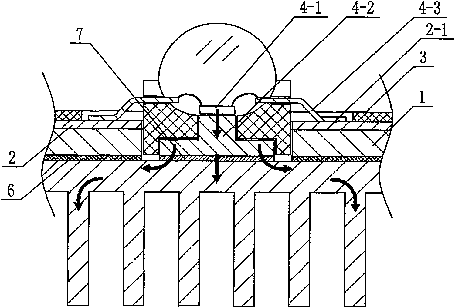
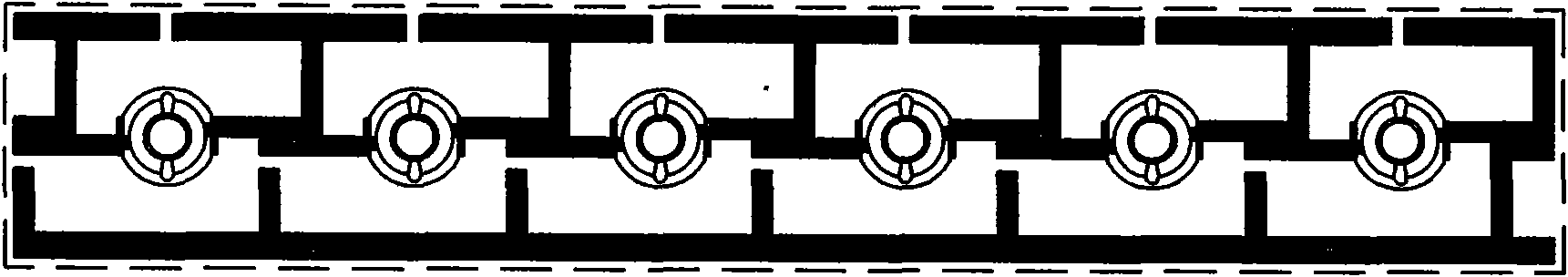
[0035] 1. Select a thin metal plate or PCB board with uniform thickness as the substrate 1, arrange the copper foil connection circuit 2 on the front of the substrate 1 by bonding and bonding, and spray transparent insulating glue on the surface of the substrate 1 and the connection circuit 2 to form bonding or thermocompression bonding The insulating coating layer 3 constitutes the LED circuit board, and the LED circuit board is provided with holes for accommodating LED light sources in a certain order. The exposed LED connection pad 2 - 1 and the external circuit connection pad 2 - 2 are left beside the position of the insulating film layer 3 covering the connection circuit 2 .
[0036] 2. Solder and connect the pin 4 of the LED light source to the connection circuit 2 on the LED circuit board through the exposed LED connection pad 2-1 next to the insulating coating layer 3 .
[0037] 3. The heat sink 5 is made of a metal material with low thermal resistance, high thermal co...
Embodiment 2
[0039] 1. Select any one of resin material film, rubber material sheet or plastic metal film with uniform thickness with certain bending, twisting and curling properties as the substrate 1, and connect the conductive film connecting circuit 2 to the front of the substrate 1 by bonding 1. Spraying transparent insulating glue on the surface of the substrate 1 and the connection circuit 2 for bonding or thermocompression bonding to form an insulating coating layer 3 to form an LED circuit board. The LED circuit board is provided with LED light source accommodation holes in a certain order. The exposed LED connection pad 2 - 1 and the external circuit connection pad 2 - 2 are left beside the position of the insulating film layer 3 covering the connection circuit 2 .
[0040] 2. Solder and connect the pin 4 of the LED light source to the connection circuit 2 on the LED circuit board through the exposed LED connection pad 2-1 next to the insulating coating layer 3 .
[0041] 3. The ...
PUM
 Abstract
Description
Claims
Application Information
 - R&D
- Intellectual Property
- Life Sciences
- Materials
- Tech Scout
- Unparalleled Data Quality
- Higher Quality Content
- 60% Fewer Hallucinations
Browse by: Latest US Patents, China's latest patents, Technical Efficacy Thesaurus, Application Domain, Technology Topic, Popular Technical Reports.
© 2025 PatSnap. All rights reserved.Legal|Privacy policy|Modern Slavery Act Transparency Statement|Sitemap|About US| Contact US: help@patsnap.com