Method for reducing formation of crystal lattice defect of chip welding disk area and corresponding welding disk forming method

A chip pad and lattice defect technology, which is applied in the field of chip pad formation, can solve the problems of unreliable time control methods, no effective prevention of lattice defects, etc., so as to avoid lattice defects, improve conductivity and The effect of reliability

Active Publication Date: 2012-05-09
SEMICON MFG INT (SHANGHAI) CORP
View PDF3 Cites 0 Cited by
  • Summary
  • Abstract
  • Description
  • Claims
  • Application Information

AI Technical Summary

Problems solved by technology

[0004] Existing technologies often use time control to prevent the appearance of lattice defects, but this method of controlling time is not reliable; therefore, in the prior art, organic solvent cleaning and plasma sputtering are more used after lattice defects appear. remove it by shooting
In this way, there is no effective prevention of the occurrence of lattice defects

Method used


Image

  • Method for reducing formation of crystal lattice defect of chip welding disk area and corresponding welding disk forming method
  • Method for reducing formation of crystal lattice defect of chip welding disk area and corresponding welding disk forming method
  • Method for reducing formation of crystal lattice defect of chip welding disk area and corresponding welding disk forming method

Examples


Embodiment Construction

[0028] In order to make the purpose and features of the present invention more comprehensible, the specific implementation manners of the present invention will be further described below in conjunction with the accompanying drawings.

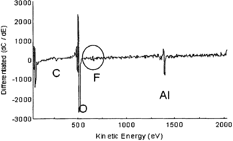
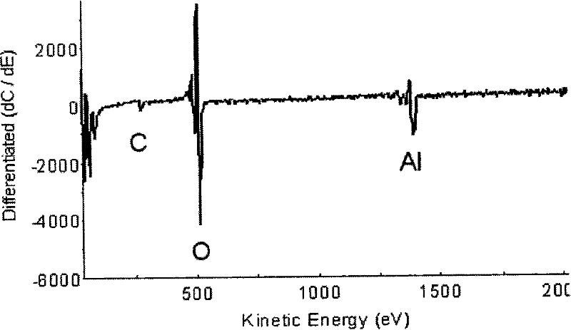
[0029] Please refer to figure 1 , which is a schematic flowchart of a method for forming a chip pad provided by an embodiment of the present invention. As shown in the figure, this method adds an argon sputtering step in the pad formation process to remove the fluorine-containing thin layer formed on the surface of the conductive layer during the patterning process to avoid the fluorine ion in the fluorine-containing thin layer Formation of lattice defects due to escape. It specifically includes the following steps:

[0030] S1: Deposit a conductive layer on the chip substrate,

[0031] Wherein the conductive layer is usually an aluminum layer or an aluminum alloy layer;

[0032] S2: Coating photoresist on the conductive layer;

[0033] S3...


PUM


Abstract

The invention discloses a method for reducing the formation of crystal lattice defects of a chip welding disk area and a corresponding welding disk forming method, which use argon plasma sputtering to remove a fluorine-contained thin layer formed on the surface of a conducting layer in the composition process of the conducting layer, thereby preventing the formation of the crystal lattice defectscaused by the effusion of fluorine ions in the fluorine-contained thin layer and improving the electrical conductivity and the reliability of a welding disk.

Description

technical field [0001] The invention relates to a method for forming a chip pad (PAD), in particular to a method for reducing the formation of lattice defects in the pad area during the etching process of the chip pad. Background technique [0002] In the chip manufacturing process, it is often necessary to connect the components formed in each film layer together to form a complete semiconductor device, or to connect the semiconductor device with other electronic components to form the required electronic circuit module; to complete these connections It is necessary to form many pads (PAD), and it can be said that the pad is an important connection member in the chip manufacturing process. For this reason, the pad has higher requirements on conductivity and reliability. Therefore, aluminum or aluminum alloy is often used to construct its conductive layer. [0003] However, in the existing pad formation process, since fluorine-containing etching gas is used to pattern the ...

Claims


Application Information

Patent Timeline
Patent Type & Authority Patents(China)
IPC IPC(8): H01L21/60H01L21/3213
Inventor 代大全张校平傅海林吴齐
Owner SEMICON MFG INT (SHANGHAI) CORP
Why Eureka
Try Eureka