
A needle tracking inspection device, a detecting device and a needle tracking inspection method

An inspection device and inspection method technology, applied in the direction of measuring device, using optical device, optical testing defect/defect, etc., can solve the problem of inability to distinguish chip shadow 112 and exposed area 111, chip unqualified, etc., and achieve rapid abnormality , The effect of good precision and reliable precision

Active Publication Date: 2009-12-02
TOKYO ELECTRON LTD
View PDF4 Cites 4 Cited by
  • Summary
  • Abstract
  • Description
  • Claims
  • Application Information

AI Technical Summary

Problems solved by technology

Therefore, in the case of determining the exposed area 111 using existing devices, as Figure 23 shown, from Figure 23 The black and white image of (a) is obtained Figure 23 In the binarized image shown in (b), the shadow 112 and exposed area 111 of cutting chips cannot be distinguished
Therefore, there is a problem that the exposed area 111 is misrecognized as the shadow 112 of the chip, and the chip on which the exposed area 111 is formed is judged to be a good product, or conversely, the shadow 112 of the chip is misidentified as the exposed area. 111. It is determined that the chip that is a qualified product is a defective product, so it is difficult to judge whether an exposed area 111 is formed on the electrode pad 100 by the control unit

Method used


Image

  • A needle tracking inspection device, a detecting device and a needle tracking inspection method
  • A needle tracking inspection device, a detecting device and a needle tracking inspection method
  • A needle tracking inspection device, a detecting device and a needle tracking inspection method

Examples


no. 1 approach

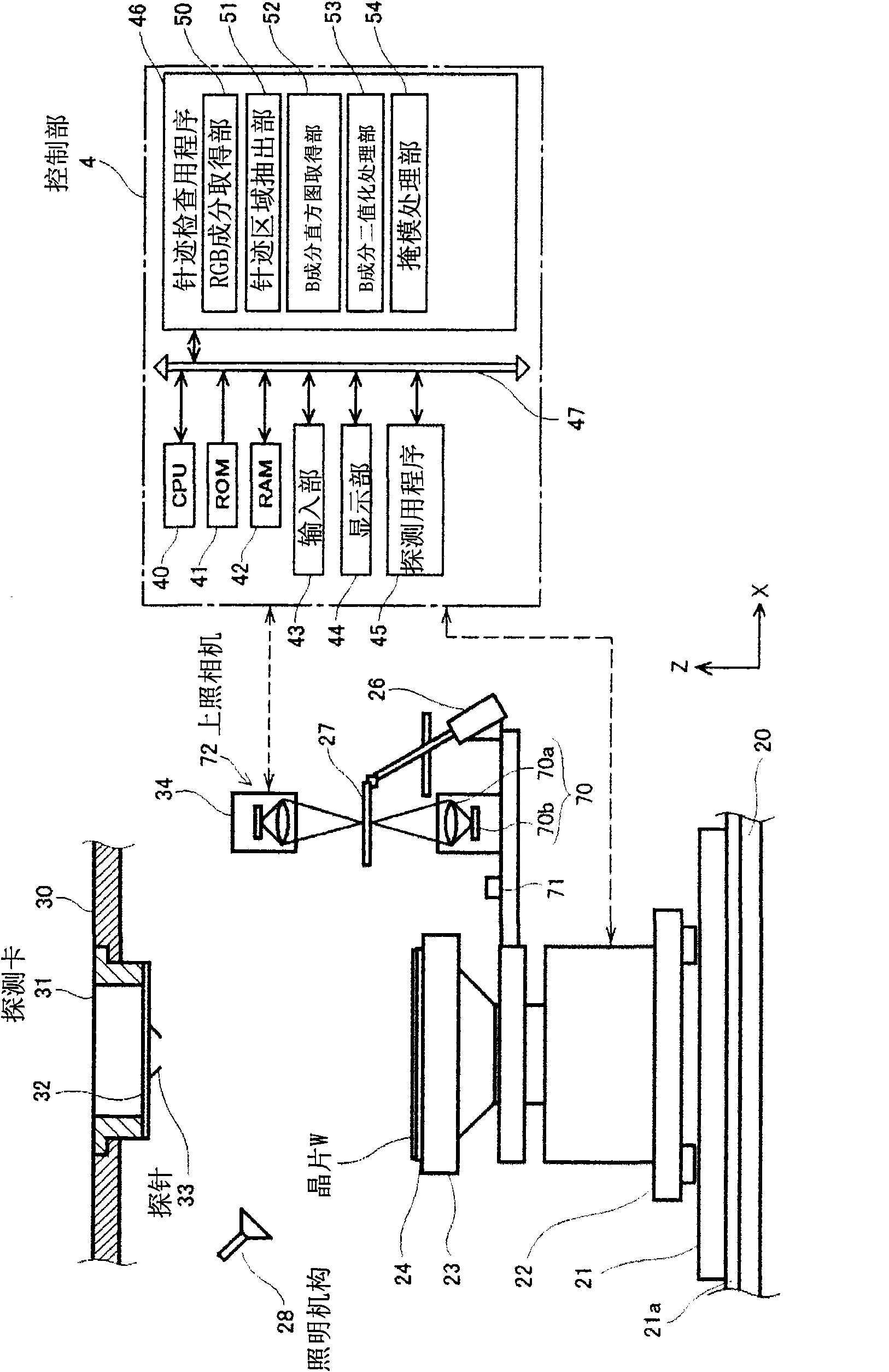
[0104] figure 1 It is a figure which shows the detection apparatus which incorporates the stitch inspection apparatus which concerns on embodiment of this invention. This detection device has a base 20 on which a first table 21 is mounted in a state of being movably supported on a first guide rail 21 a extending in parallel in the X direction, and passes through the first table through an axis. A ball screw and a motor (not shown) of the stage 21 can move in the X direction shown in the figure. In addition, on the first table 21, like the first table 21, the second table 22 is placed so as to be movable in the Y direction (not shown) perpendicular to the X and Z directions. On the second table 22 is placed a third table 23 that can move in the illustrated Z direction by a motor not shown.

[0105] On the moving body of the third workbench 23, a top suction cup (Chuck top) 24 as a mounting table is provided, which takes the Z-axis as the rotation center and has only a slight...

no. 2 approach

[0137]The present invention is a stitch inspection device which obtains a color image of an electrode pad, obtains an image corresponding to the R, G, and B components of the image, and utilizes the reflectance of the electrode pad and the reflection of the base film in the component data. Among these components, the difference in rate is the largest in the component data, and the exposed area is detected. Therefore, the imaging mechanism of the wafer W is not limited to the upper camera 72 of the first embodiment, and for example, another dedicated camera may be installed at a different position from the upper camera 72, for example, on the top plate or the like. In addition, as an imaging mechanism, it is not limited to a color camera capable of acquiring color images including R, G, and B components like the upper camera 72, and for example, three cameras that exclusively acquire R, G, and B components may be combined to form an imaging mechanism. mechanism.

[0138] Based...

no. 3 approach

[0141] In addition, as an embodiment of the present invention, the form shown in the following third embodiment is also possible. In the detecting device of the third embodiment, instead of the upper camera 72 and the lighting mechanism 28 provided in the first embodiment, a Figure 15 The shown upper camera 72m capable of acquiring imaging data D1 as a black-and-white image is further provided with R illuminating means 28r, G illuminating means 28g, and B illuminating means 28b for illuminating wafer W, which are composed of, for example, light emitting diodes. The R illumination mechanism 28r illuminates the wafer W with red light, the G illumination mechanism 28g illuminates the wafer W with green light, and the B illumination mechanism 28b illuminates the wafer W with blue light. As a result, in the upper camera 72m, only the image data of the components corresponding to the light sequentially irradiated from the respective illumination mechanisms 28r, 28g, and 28b can be ...


PUM


Abstract

The invention provides a needle tracking inspection device, a detecting device with the device and a needle tracking inspection method that can detect protrusion condition of a base layer of an electrode mat to a cardinal plate after detection automatically with high precision, wherein the needle tracking inspection device comprises the following procedures: obtain a R ingredient data (D2), a G ingredient data (D3) and a B ingredient data (D4), then a RGB ingredient obtaining part (50) of the B ingredient data (D4) is selected according to the difference of the reflection index of material quality of an electrode mat (2) and that of a basal layer (6); and to the B ingredient data (D4), in order to obtain image of the basal layer (6) distinguished from the electrode mat (2), a set grey level and a B ingredient histogram obtaining part (52) as relation data having pixels of the grey level, then according to the obtained histogram judge the existence of protrusion of the basal layer (6) in the needle tracking.

Description

technical field [0001] The present invention relates to a stitch inspection device, a stitch inspection method, and a detection device provided with the stitch inspection device, which automatically detect exposure conditions such as the presence or absence of a base layer of electrode pads on a substrate after probe inspection. Background technique [0002] Conventionally, a probe device is used as a device for measuring electrical characteristics of an IC chip formed on a semiconductor substrate. The probing device includes a table on which the substrate is placed and can move freely in three-dimensional directions, and a probe card. A so-called probe test is performed in which the probes of the probe card come into contact with electrode pads that are connected to the wiring on the substrate. Pattern connection, thereby performing electrical measurements of the chip. [0003] Generally, a probe is used as a probe, and an overdrive is applied in order to scrape off the na...

Claims


Application Information

Patent Timeline
IPC IPC(8): H01L21/66G01N21/88G01B11/22
CPCG01N21/8851G01N21/95684G01N2021/8887
Inventor 梅原康敏月嶋慎河野功佐野聪
Owner TOKYO ELECTRON LTD
Learn More