Active element matrix substrate

An active element and matrix technology, applied in nonlinear optics, instruments, optics, etc., can solve problems such as the decrease of pixel aperture ratio and affect the brightness performance of LCD 100, so as to increase the aperture ratio, avoid light leakage, and improve the pixel aperture ratio Effect

Active Publication Date: 2011-05-04
AU OPTRONICS CORP
View PDF0 Cites 0 Cited by
  • Summary
  • Abstract
  • Description
  • Claims
  • Application Information

AI Technical Summary

Problems solved by technology

However, widening the width W' of the black matrix 124 will reduce the pixel aperture ratio (Aperture Ratio) of the liquid crystal display panel 150, thereby affecting the brightness performance of the liquid crystal display 100.

Method used


Image

  • Active element matrix substrate
  • Active element matrix substrate
  • Active element matrix substrate

Examples


no. 1 example

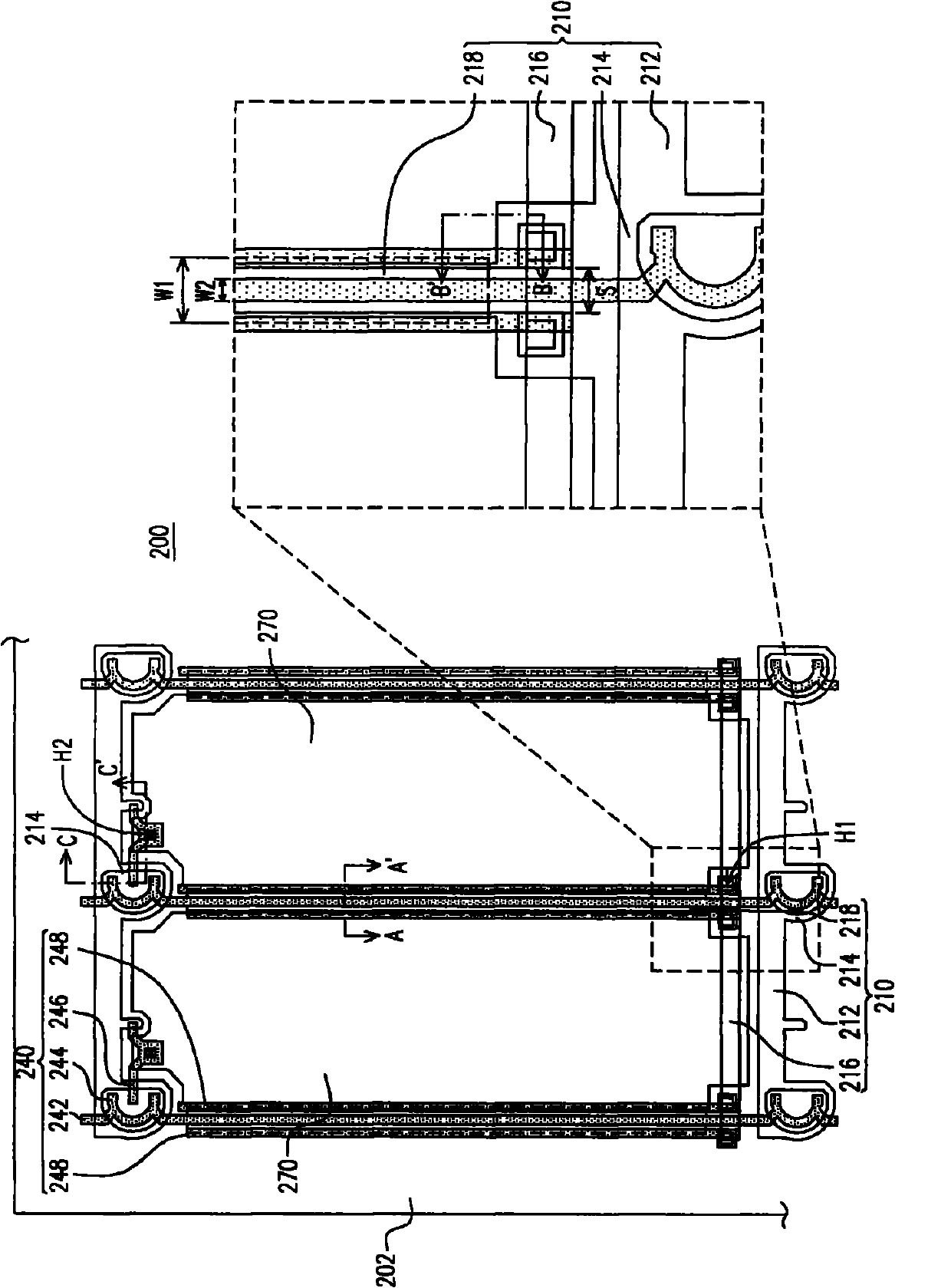
[0072] figure 2 It is a partial top view of an active element matrix substrate according to the first embodiment of the present invention, Figure 3A will be figure 2 The partial cross-sectional view of the active element matrix substrate applied to the liquid crystal display in Figure 3A The position of the mid-section is roughly along the figure 2 The corresponding position of the active element matrix substrate 200 of the cross-section line AA' in the middle. Please also refer to figure 2 and Figure 3A The active device matrix substrate 200 of this embodiment includes a substrate 202 , a first patterned conductor layer 210 , a dielectric layer 230 , a second patterned conductor layer 240 , a protection layer 260 and a plurality of pixel electrodes 270 .

[0073] Please also refer to figure 2 and Figure 3A , the first patterned conductor layer 210 is disposed on the substrate 202, the first patterned conductor layer 210 includes a plurality of scanning lines 2...

no. 2 example

[0086] Figure 4 It is a partial top view of an active element matrix substrate according to the second embodiment of the present invention, please refer to Figure 4 The active element matrix substrate 400 of this embodiment is similar to the active element matrix substrate 200 of the first embodiment. In the pixel unit of the active element matrix substrate 400 of this embodiment, the storage capacitor is in the form of a storage capacitor on the scanning line 212 type (Cst on scan line). For clarity, the same components in this embodiment and the first embodiment are denoted by the same symbols.

[0087] Figure 5 for Figure 4 Schematic cross-section along the section line BB'. Please refer to Figure 5 , in this embodiment, the position of the first contact opening H1 of the dielectric layer 230 is opened above the scan line 212 , in other words, the first contact opening H1 respectively exposes a part of the scan line 212 . Moreover, each strip capacitor electrode ...


PUM


Abstract

The invention discloses to an active element matrix substrate. The substrate comprises a first patterning conductor layer, a dielectric layer, a second patterning conductor layer, a protective layer and a plurality of pixel electrodes, wherein the first patterning conductor layer comprises a plurality of scanning lines and common lines, a plurality of grid electrodes and a strip floating shading pattern; the dielectric layer covers the first patterning conductor layer and is provided with a plurality of contact openings which expose the common lines respectively; the second patterning conductor layer comprises a plurality of data wires, a plurality of source electrodes and drain electrodes, and a plurality of strip capacitance electrodes; each strip capacitance electrode is in electrical connection with one common line through one first contact opening; a clearance is reserved between each data wire and one strip capacitance electrode; each strip floating shading pattern is positionedbelow the data wire, the clearance and the strip capacitance electrode; and the pixel electrodes are in electrical connection with the drain electrodes through second contact openings of the protective layer.

Description

technical field [0001] The present invention relates to a substrate, and in particular to an active element matrix substrate. Background technique [0002] Among many Flat Panel Displays (FPDs), Liquid Crystal Displays (LCDs) have become the mainstream in the current market because of their superior characteristics such as high space utilization efficiency, low power consumption, no radiation, and low electromagnetic interference. [0003] Figure 1A It is a three-dimensional schematic diagram of a liquid crystal display in the prior art. Please refer to Figure 1A The liquid crystal display 100 has an active element matrix substrate 110 , an opposite substrate 120 , a liquid crystal layer 130 interposed between the active element matrix substrate 110 and the opposite substrate 120 , and a backlight module 140 for providing light. The active device matrix substrate 110 has a plurality of pixel units 112 and a plurality of signal lines 114 between the pixel units 112 , and t...

Claims


Application Information

Patent Timeline
Patent Type & Authority Patents(China)
IPC IPC(8): G02F1/1362G02F1/133
Inventor 刘竹育施明宏吴宙秦陈怡君
Owner AU OPTRONICS CORP
Why Eureka
Try Eureka