CMOS image sensing component

An image sensing element and semiconductor technology, which is applied in the direction of semiconductor devices, electrical components, electric solid devices, etc., can solve the problems of crossing interference, limited effect, loss of incident light photon number, etc., and achieve the effect of avoiding crossing interference

Inactive Publication Date: 2006-11-01
UNITED MICROELECTRONICS CORP
View PDF0 Cites 0 Cited by
  • Summary
  • Abstract
  • Description
  • Claims
  • Application Information

AI Technical Summary

Problems solved by technology

However, when the depletion region is irradiated with incident light and converts photons into electric current, the number of photons of incident light will be lost with the incident depth, especially for short-wavelength light (such as blue light), because short-wavelength light is harmful to the semiconductor wafer. The skin penetration depth (skin depth) is shallower, and its sensitivity attenuation will be more serious
On the other hand, since the junction current induced by the depletion region is also located deep in the substrate 12, the effect of the P-type well 13 in blocking the lateral drift of the junction current is limited, which easily leads to the occurrence of cross talk.

Method used


Image

  • CMOS image sensing component
  • CMOS image sensing component
  • CMOS image sensing component

Examples


Embodiment Construction

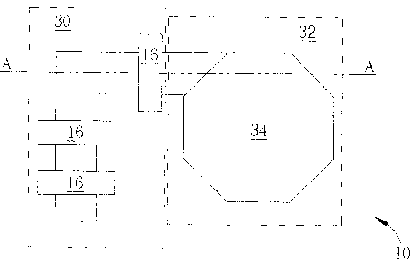
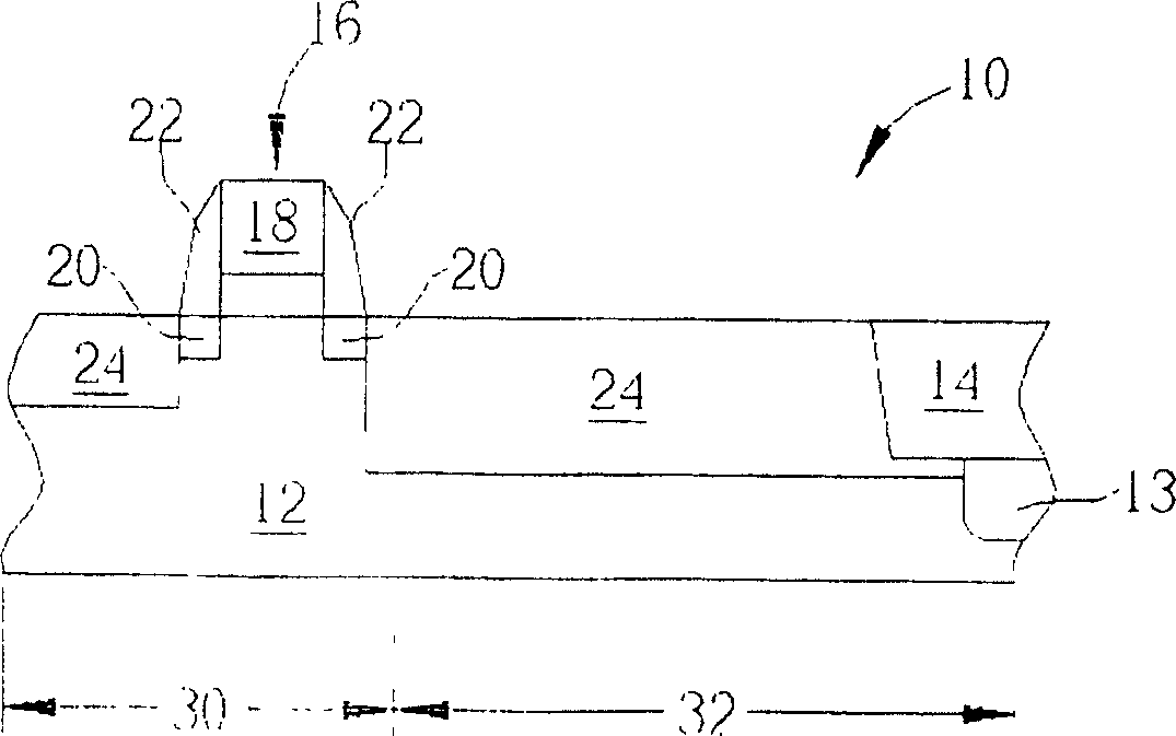
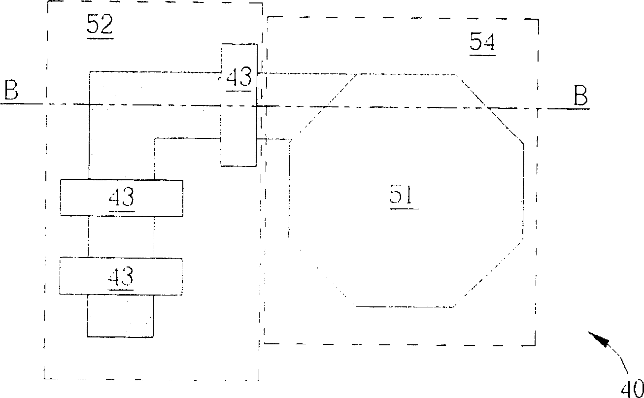
[0025] see image 3 as well as Figure 4 , image 3 It is a top view (top-view diagram) of a semiconductor wafer of a CMOS image sensor of the present invention, Figure 4 for image 3 A cross sectional diagram of the semiconductor wafer along the BB direction. The CMOS image sensor of the present invention includes three MOS transistors, which are respectively used as a reset element (reset MOS), a current source follower (current source follower), and a row selector (row selector), and a photodiode for Sensing the intensity of light.

[0026] like image 3 and Figure 4 As shown, in the preferred embodiment of the present invention, the image sensor is made on a semiconductor wafer 40 of a p-type substrate 42, and an N-channel MOS region 52 is set on the surface of the p-type substrate 42 for making The NMOS transistor 43 and a light-sensing region 54 are used to make a photodiode 51 . like Figure 4 As shown, the light-sensing region 54 in the image sensing device ...


PUM


Abstract

The invention provides a complementary metal oxide semiconductor image sensor (CMOS image sensor). The image sensor is fabricated on a semiconductor wafer, and the surface of the semiconductor wafer includes a silicon substrate of a first conductivity type. The image sensing element includes: a photo-sensing region, which is composed of a lightly doped region of a second conductivity type, and the lightly doped region is formed at a first predetermined depth on the surface of the substrate; a second predetermined depth A deep insulating layer is arranged on the surface of the substrate and surrounds the light sensing region, and the second predetermined depth is greater than the first predetermined depth; a metal oxide semiconductor transistor (MOS transistor) is fabricated on the semiconductor wafer and electrically connected to the photo-sensing region; and a deeply doped region of the first conductivity type is formed in the substrate under the insulating layer, and the dopant concentration and depth of the deeply doped region are in a Gauss distribution.

Description

technical field [0001] The present invention relates to the field of semiconductor manufacturing technology, especially a complementary metal oxide semiconductor image sensor (CMOS image sensor), especially a complementary type that can increase quantum efficiency (quantumefficiency) and avoid the phenomenon of cross talk Metal oxide semiconductor image sensor (CMOS image sensor). Background technique [0002] Solid-state image sensing devices, such as charge-coupled devices (CCDs) and CMOS images sensors, are commonly used as input devices for electronic images today. Since the CMOS image sensor is manufactured by conventional semiconductor process, it has the advantages of lower manufacturing cost and smaller device size. CMOS image sensors are used in a wide range of applications, including personal computer cameras (PC cameras) and digital cameras (digital cameras). [0003] see figure 1 as well as figure 2 , figure 1 It is a top-view diagram of a semiconductor waf...

Claims


Application Information

Patent Timeline
Patent Type & Authority Patents(China)
IPC IPC(8): H01L27/14H01L27/146H01L27/148
CPCH01L27/14601H01L27/14603H01L27/1463
Inventor 陈重尧林震宾
Owner UNITED MICROELECTRONICS CORP
Why Eureka
Try Eureka