Safety JTAG module and method for protecting safety of information inside chip

A safe and secure configuration technology, applied in computer security devices, internal/peripheral computer component protection, instruments, etc., can solve the problem of not being able to access the content that user B can access, inconvenient for personalized distribution and multi-party development, and JTAG port protection measures failure and other problems, to achieve personalized management, avoid the risk of failure, and ensure the effect of safety

Inactive Publication Date: 2010-01-06
SHENZHEN STATE MICRO TECH CO LTD
View PDF5 Cites 44 Cited by
  • Summary
  • Abstract
  • Description
  • Claims
  • Application Information

AI Technical Summary

Problems solved by technology

The existing technology has considered the potential safety hazards of SOC chip debugging, but the overall safety of the test is insufficient.
[0005] For example, the Chinese patent applications with application numbers 200410003197 and 200610050898 respectively provide a technical solution to solve the above-mentioned potential safety hazard caused by the JTAG port from the perspective of chip debugging, but there are the following defects: the technical solutions provided by these two patent applications It is suitable for one-time mass programming, and it is not convenient for personalized distribution and multi-party development; the personalized distribution here means that in the case of JTAG protection, user A can only access the content that user A can access through the JTAG port, but cannot access The content that user B can access; In addition, these two patent applications only provide two options: off or on, and do not use the tracking and analysis of chip failures after productization
The user may even open the closed JTAG port through the full scan chain test technology, thereby invalidating the JTAG port protection measures

Method used


Image

  • Safety JTAG module and method for protecting safety of information inside chip
  • Safety JTAG module and method for protecting safety of information inside chip
  • Safety JTAG module and method for protecting safety of information inside chip

Examples


Embodiment Construction

[0045] Specific embodiments of the present invention will be described below in conjunction with the accompanying drawings.

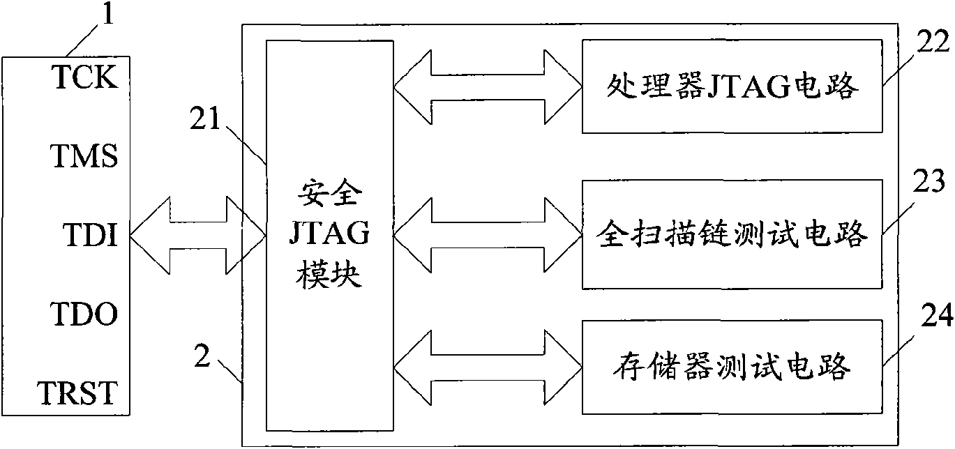
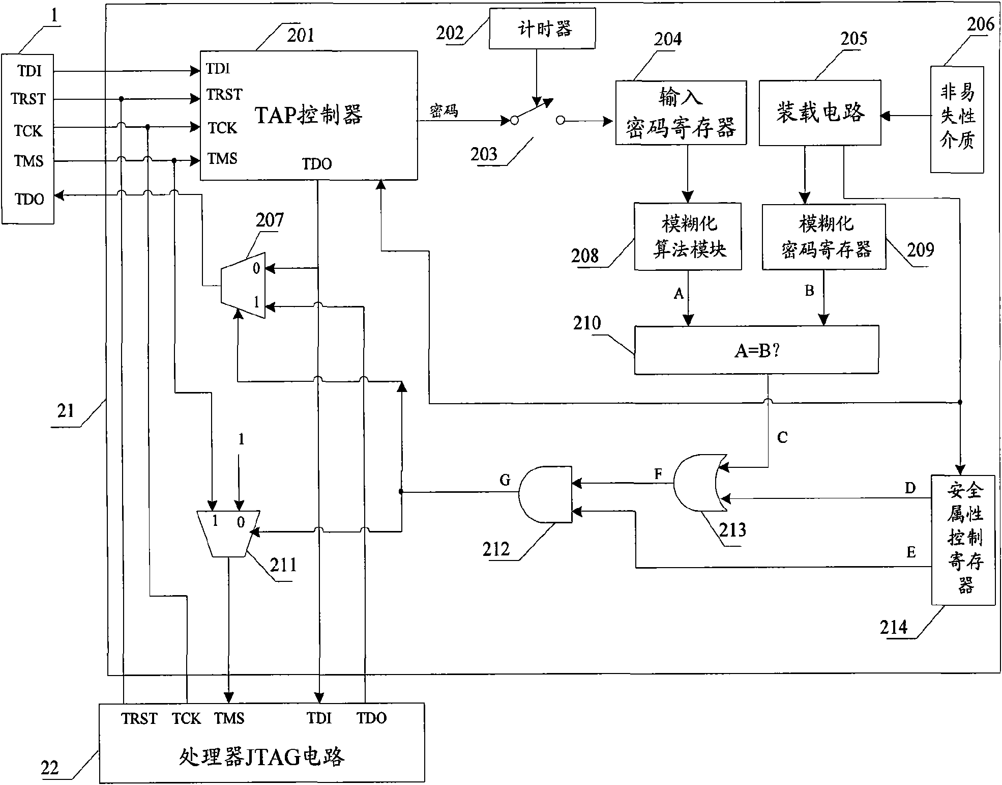
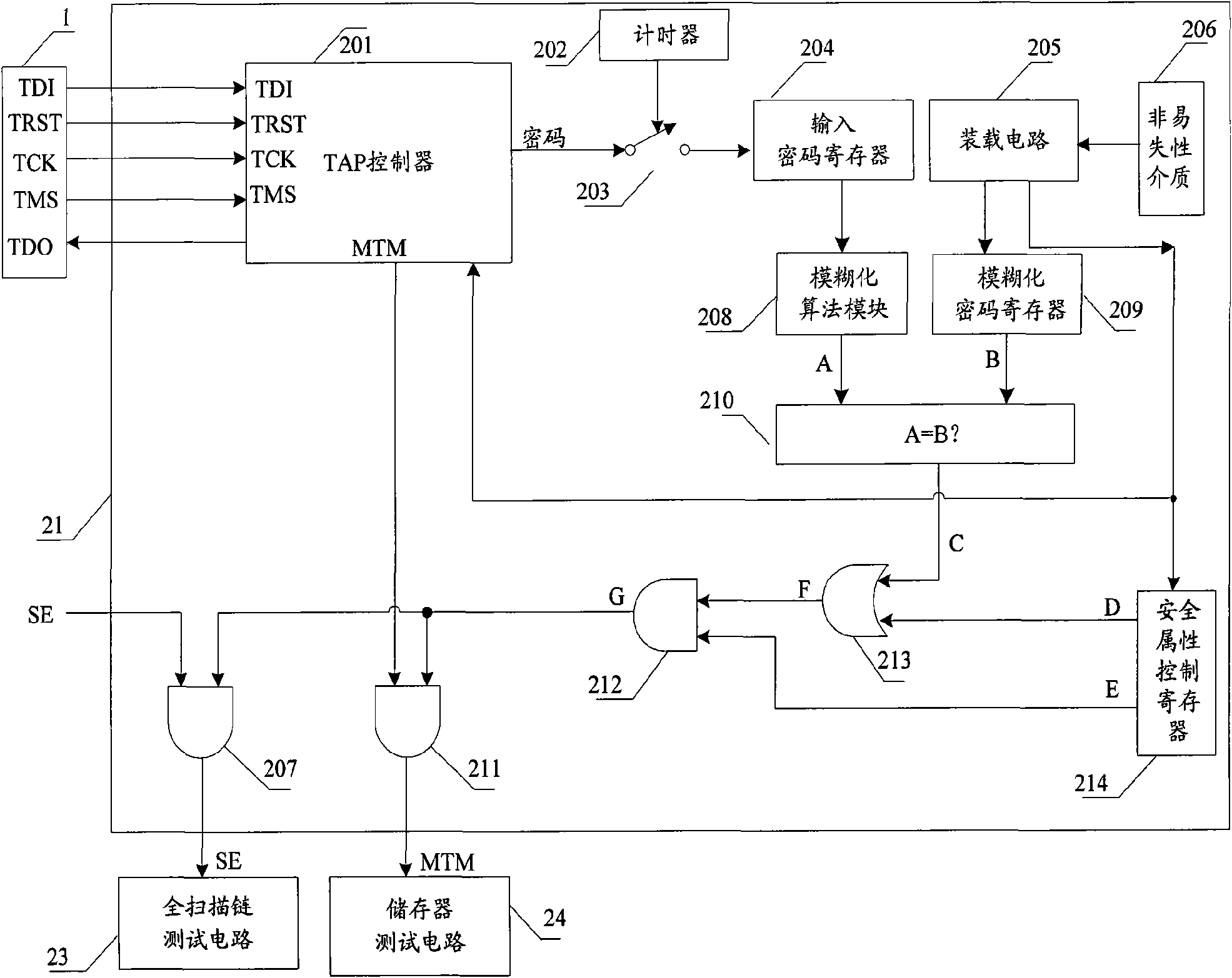
[0046] figure 1 It is a schematic diagram of the internal structure of the system chip disclosed in the present invention. A system on chip (System on Chip, SOC) 2 includes: a security JTAG (Join Test Action Group) module 21 , a processor JTAG circuit 22 , a full scan chain test circuit 23 and a memory test circuit 24 . Processor JTAG circuit 22, full scan chain test circuit 23 and memory test circuit 24 are the object (abbreviation protection object) that system chip 2 is protected by safety JTAG module 21, only through the safety permission of safety JTAG module 21, the user just can pass through JTAG port 1 accessing or starting the protection object, and realizing the test or debugging of the system chip 2 . Therefore, the present invention focuses on describing how the security JTAG module 21 implements security control on the processor JTAG circ...


PUM


Abstract

The invention relates to a safety JTAG module and a method for protecting security of information inside a chip, wherein the safety JTAG module comprises a nonvolatile medium (206), a loading circuit (205), a security attribute control register (214), a TAP controller (201), two selectors (207 and 211), a switch (203), a password authentication module and a logic processing module; the TAP controller (201) and the two selectors (207 and 211) are connected between a JTAG port (1) and a protected object inside the chip; the switch (203) is switched by the control of a timer (202); the password authentication module is used for authenticating whether a clear-text password input by a user is accordant with a fuzzification password or not; and the logic processing module is used for logically processing an authentication result output by the password authentication module and an indication signal output by the security attribute control register (214) and outputting an enable signal to the two selectors (207 and 211) so as to control whether the JTAG port (1) is allowed to be connected with the protected object inside the chip through the TAP controller (201) or not. The invention ensures the security and the convenience of an SOC chip in testing and debugging processes, thereby protecting the security of data inside the chip.

Description

technical field [0001] The present invention relates to the security control technology of SOC chip JTAG port, especially relate to a kind of security JTAG module that carries out security control to processor JTAG circuit, memory test circuit and full scan chain test circuit inside SOC chip, and application of the security JTAG Module to realize the method of protecting the internal information security of the chip. Background technique [0002] Testing and debugging is an important link in the design and production of SOC (System-on-Chip) chips. The test is used to ensure that the SOC chip can work normally, and the purpose of debugging is mainly to facilitate the application development or fault tracking analysis of the chip. [0003] For the debugging of the integrated processor (central processing unit, microprocessor) of the SOC chip, the JTAG (Join Test Action Group) port is mainly used. The user can control the processor to execute the instruction expected by the u...

Claims


Application Information

Patent Timeline
Patent Type & Authority Applications(China)
IPC IPC(8): G06F21/00G06F21/71
Inventor 王良清张鹏
Owner SHENZHEN STATE MICRO TECH CO LTD
Why Eureka
Try Eureka