Device and method for detecting lens aberration of lithography machines

A detection device and lithography machine technology, which is applied in the direction of photolithography exposure device, micro-lithography exposure equipment, etc., can solve the problem that the defect in the local area of ​​the lens is difficult to be found, the problem of the lens of the lithography machine equipment is found, and all parts are detected and other problems to achieve the effect of improving monitoring capabilities, shortening detection time, and simplifying detection steps

Active Publication Date: 2011-06-22
SHANGHAI HUAHONG GRACE SEMICON MFG CORP
View PDF0 Cites 0 Cited by
  • Summary
  • Abstract
  • Description
  • Claims
  • Application Information

AI Technical Summary

Problems solved by technology

In actual semiconductor companies, the lens aberration of the lithography machine is usually detected once every six months or a year, which is not conducive to the timely detection of lens problems of the lithography machine equipment
[0010] At the same time, the existing method measures the lens aberration through some specific test patterns, which does not guarantee that all parts of the lens can be detected, and different aberration results are often obtained for test patterns of different processes. Defects are hard to spot

Method used


Image

  • Device and method for detecting lens aberration of lithography machines
  • Device and method for detecting lens aberration of lithography machines
  • Device and method for detecting lens aberration of lithography machines

Examples


Embodiment Construction

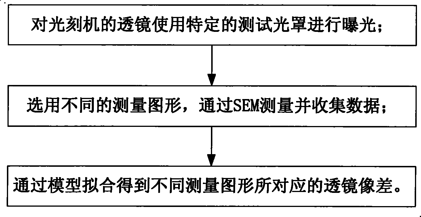
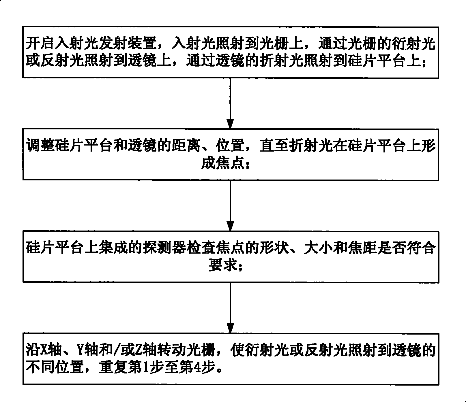
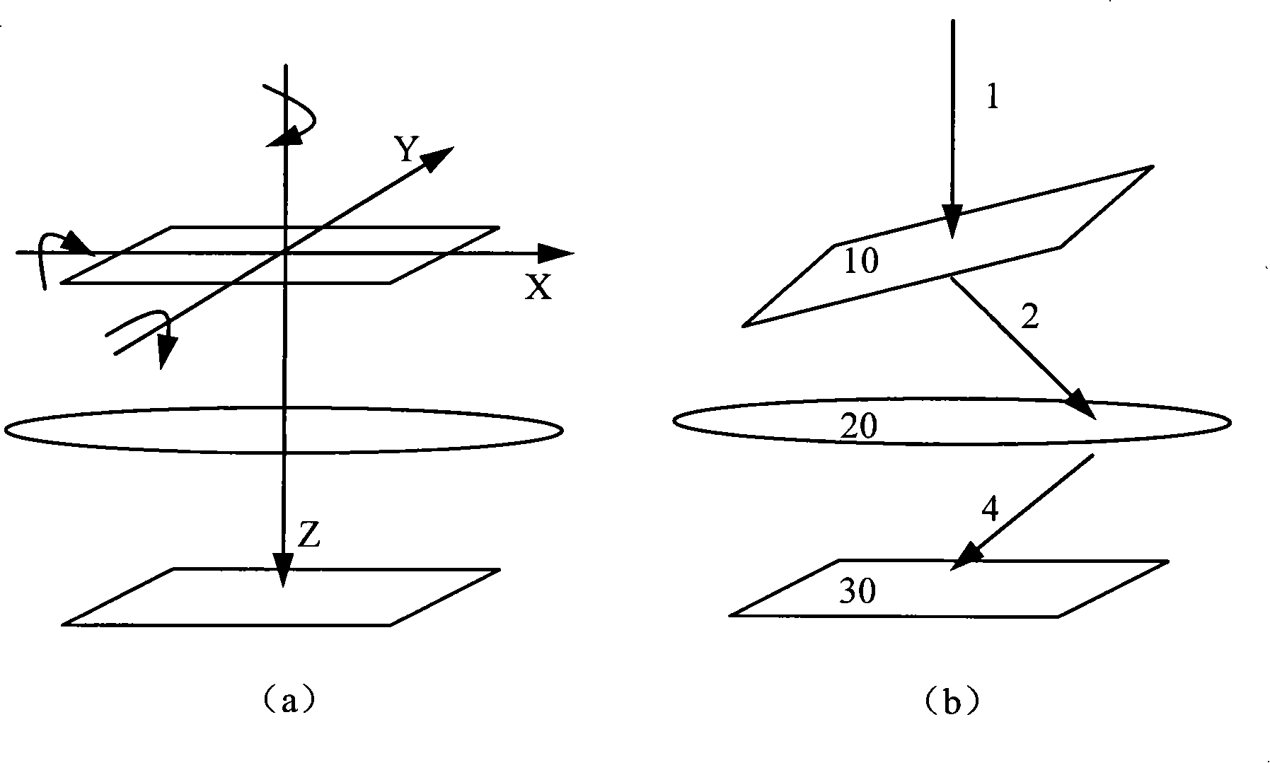
[0030] see image 3 (b), the detection device of the lens aberration of the lithography machine of the present invention comprises:

[0031] An incident light generating device (not shown), emitting incident light 1;

[0032] An imaging lens 20, the main lens of the photolithography machine is selected;

[0033] A transmission grating 10 and a silicon wafer platform 30, the grating 10 and the silicon wafer platform 30 are respectively placed on both sides of the optical path of the lens 20;

[0034] A detector (not shown), integrated on the silicon wafer platform 30 , measures the position, shape, size and focal length of the focal point formed on the silicon wafer platform 30 by the refracted light passing through the lens 20 .

[0035] see Figure 4 (b), this is another embodiment of the detection device for the lens aberration of the lithography machine of the present invention, which is the same as image 3 The difference is that the transmission grating 10 is replaced...


PUM


Abstract

The invention discloses a method for detecting lens aberration of lithography machines, which comprises: step 1, an incident light generating device is turned on; incident light is radiated onto a grating; diffraction light or reflected light through the grating is radiated onto a lens; and refracted light through the lens is radiated onto a silicon chip platform; step 2, the distance and positions of the silicon chip platform and the lens are adjusted till the refracted light forms a focus on the silicon chip platform; step 3, a detector integrated on the silicon chip platform measures the position, shape, size and focal length of the focus and judges whether the position, shape, size and focal length of the focus meet requirements; and step 4, the grating is rotated along an X axis, a Yaxis and / or Z-axis to radiate the diffraction light or the reflected light to different positions of the lens, and the step 1 to the step 4 is repeated. The invention also discloses a detection device corresponding to the method. The invention has the advantages of realizing automatic detection and monitoring of the lens aberration of lithography machines and helping improve both product yield and equipment utilization efficiency.

Description

technical field [0001] The invention relates to a detection and monitoring method for photoetching machine equipment in semiconductor manufacturing. Background technique [0002] In semiconductor manufacturing, photolithography is a key technology for pattern transfer, and the control accuracy and resolution of photolithography process directly determine the technical capabilities of semiconductor manufacturing. Among the many factors affecting the lithography process, the quality of the lithography machine lens is the fundamental factor, and the quality of imaging is directly determined by the lens. [0003] For optical lenses, due to the limitations of existing technology and materials and equipment, there must be aberrations in actual lenses, and aberration is one of the key indicators to determine whether a lens is good or bad. Common aberrations mainly include spherical aberration (non-uniform focus at the edge and middle of the lens), coma (non-uniform focus of the le...

Claims


Application Information

Patent Timeline
Patent Type & Authority Patents(China)
IPC IPC(8): G03F7/20
Inventor 王雷
Owner SHANGHAI HUAHONG GRACE SEMICON MFG CORP
Why Eureka
Try Eureka