Supercharge Your Innovation With Domain-Expert AI Agents!

Semiconductor device and bias generating circuit

A technology for generating circuits and semiconductors, which is applied in the manufacture of semiconductor devices, circuits, semiconductor/solid-state devices, etc., can solve the problems of increased circuit scale and increased circuit power consumption, and achieves improved degrees of freedom, low power consumption, and small circuits effect of scale

Active Publication Date: 2010-02-03
FUJITSU LTD
View PDF1 Cites 0 Cited by
  • Summary
  • Abstract
  • Description
  • Claims
  • Application Information

AI Technical Summary

Problems solved by technology

[0008] However, if the LSI is large-scale, the substrate leakage current of the transistor will also increase, and the amount of charge required for application will also increase. However, since the above-mentioned clock application type step-up charge pump drives the capacitor to generate charge by clock application, Therefore, in order to increase the amount of charge, it is necessary to increase the number of circuits or increase the capacity of the capacitor or the clock frequency, which leads to an increase in the scale of the circuit and an increase in the power consumption of the circuit itself.
[0009] That is, in the conventional LSI having a clock application type step-up charge pump, there is a problem that the circuit scale increases or the power consumption of the circuit itself increases.

Method used


Image

  • Semiconductor device and bias generating circuit
  • Semiconductor device and bias generating circuit
  • Semiconductor device and bias generating circuit

Examples


Embodiment Construction

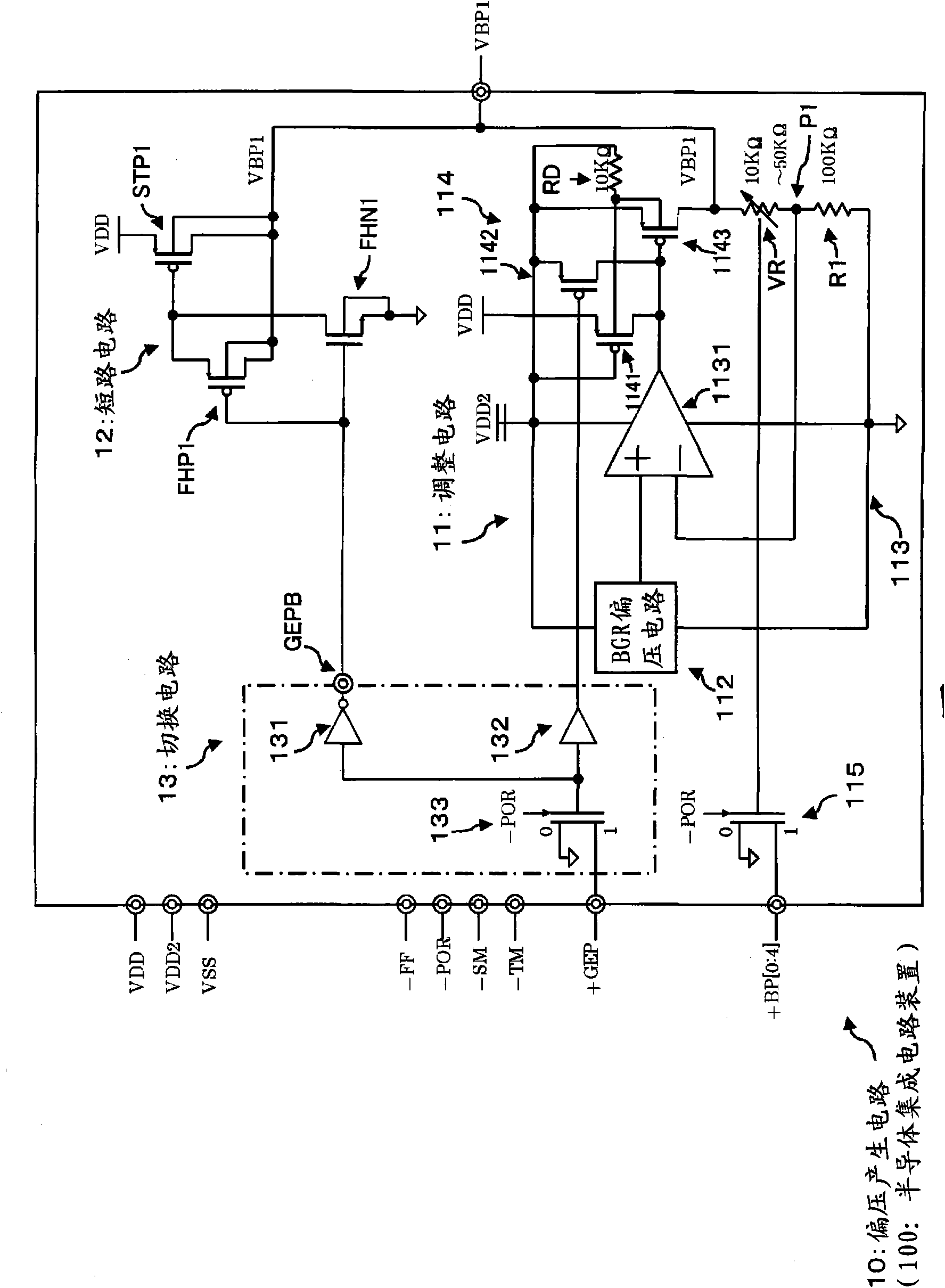
[0038] Hereinafter, embodiments of the present invention will be described with reference to the drawings.

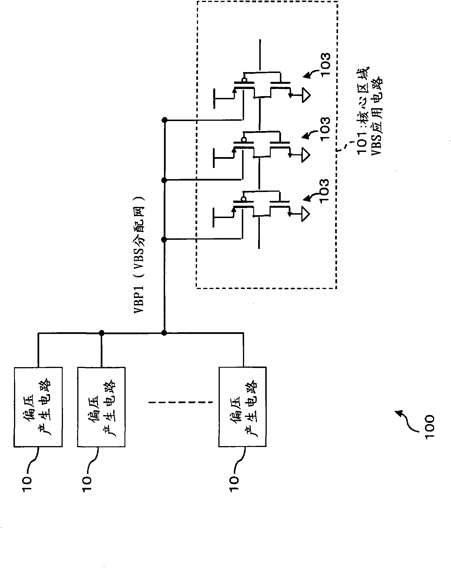
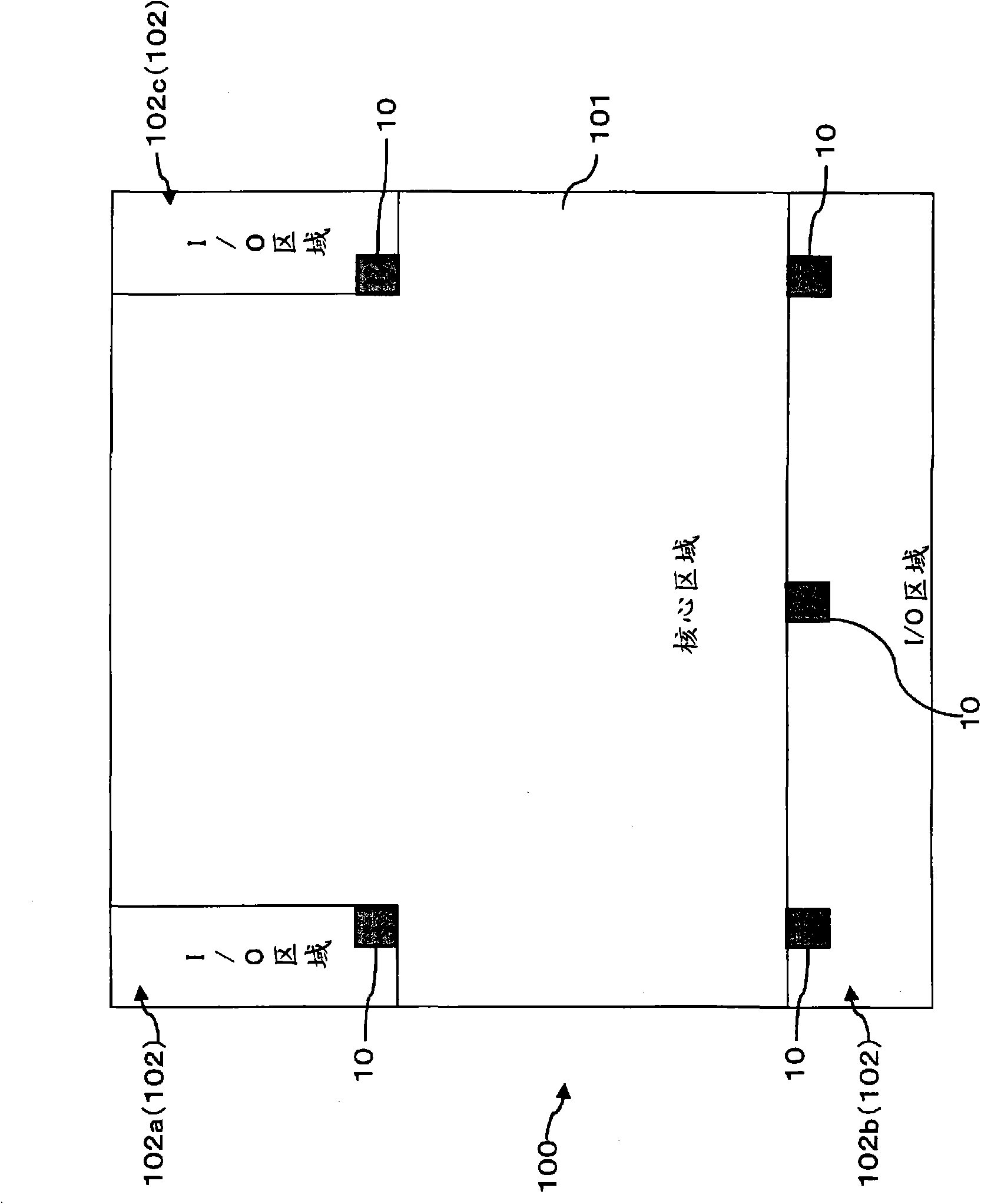
[0039] figure 1 is a circuit configuration diagram of a bias voltage generating circuit 10 according to an embodiment of the present invention, figure 2 It is a figure which shows the example of the output connection of the bias voltage generating circuit 10 in the semiconductor integrated circuit device 100, image 3 is a diagram showing an example of its arrangement, Figure 4 It is a figure showing the description of the terminals in a list.

[0040] Such as figure 2 As shown, the bias generating circuit 10 is provided in a semiconductor integrated circuit device (LSI: Large Scale Integration; semiconductor device) 100, and is connected to the core region 101 of the semiconductor integrated circuit device 100 (see figure 2 , image 3 ) used in the substrate of the PMOS transistor (transistor) 103 and generates a circuit for reverse bias voltage VBS (substrat...


PUM


Abstract

There are included a first power supply voltage input part (VDD) that can input a first power supply voltage; a second power supply voltage input part (VDD2) that can input a second power supply voltage; a regulator circuit (11) that generates a back bias voltage based on the second power supply voltage; and an output part (VBP1) that can output, as an output voltage, the back bias voltage generated by the regulator circuit (11). In this way, the generation of a board bias can be achieved with lower power consumption, while the circuit scale can be reduced.

Description

technical field [0001] The present invention relates to a technique for generating a reverse bias voltage involved in a semiconductor device having a logic circuit. Background technique [0002] In recent years, due to advances in the miniaturization of transistors, the leakage current of transistors has increased, and the power consumption of LSI (Large Scale Integration, large scale integrated circuits) has gradually increased. [0003] As one of methods for reducing the leakage current of a transistor, there is known a reverse bias control method of applying a reverse bias (reverse bias, substrate bias) voltage to a substrate of a transistor. [0004] In a conventional substrate bias generating circuit for generating this reverse bias voltage, the reverse bias voltage is generally generated by a clock application type step-up charge pump. [0005] Figure 12 , Figure 13 Each is a diagram showing a configuration example of a clock application type step-up charge pump, ...

Claims


Application Information

Patent Timeline
IPC IPC(8): H01L21/822H01L27/04
CPCH01L27/0222G05F3/205G11C11/407
Inventor 田中基之
Owner FUJITSU LTD
Features
  • R&D
  • Intellectual Property
  • Life Sciences
  • Materials
  • Tech Scout
  • Unparalleled Data Quality
  • Higher Quality Content
  • 60% Fewer Hallucinations
Learn More