

Organic electroluminescent display device
An electroluminescent display and display device technology, applied in the direction of electroluminescent light source, electric light source, identification device, etc., can solve the problems of large OFF current, low ON/OFF ratio, insufficient current for sufficient mobility supply, etc.
- Summary
- Abstract
- Description
- Claims
- Application Information
AI Technical Summary
Problems solved by technology
Method used
Image

Examples
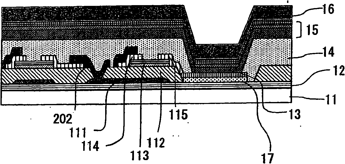
Embodiment 1
[0105] The processing conditions of each step are as follows:
[0106] Photoresist coating conditions: Photoresist OFPR-800 (manufactured by Tokyo Ohka Kogyo Co., Ltd.) was coated by spin coating at 4000 rpm for 50 sec.
[0107] 2) Formation of gate insulating film
[0108] Sputtering conditions: use RF magnetron sputtering device at 400W RF power supply and sputtering gas flow Ar / O 2 Sputtering was performed at =12.0 / 2.0 sccm.
[0109] 3) Form active layer and resistance layer
[0110] The sputtering conditions of the IGZO film with higher conductivity and the IGZO film with lower conductivity are as follows:
[0111] Sputtering conditions for IGZO films with higher conductivity: InGaZnO as target composition 4 On the polycrystalline sintered body, use the RF magnetron sputtering device at a DC power supply of 200W and a sputtering gas flow rate of Ar / O 2 Sputtering was performed at =12.0 / 0.6 sccm.
[0112] The patterning process by the photoresist method is the same as...
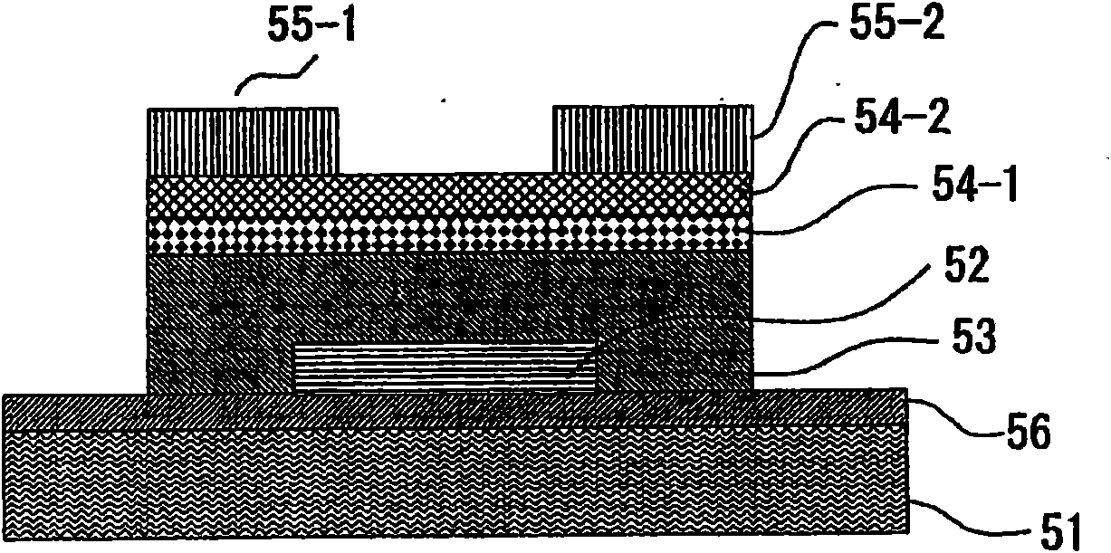
Embodiment 2
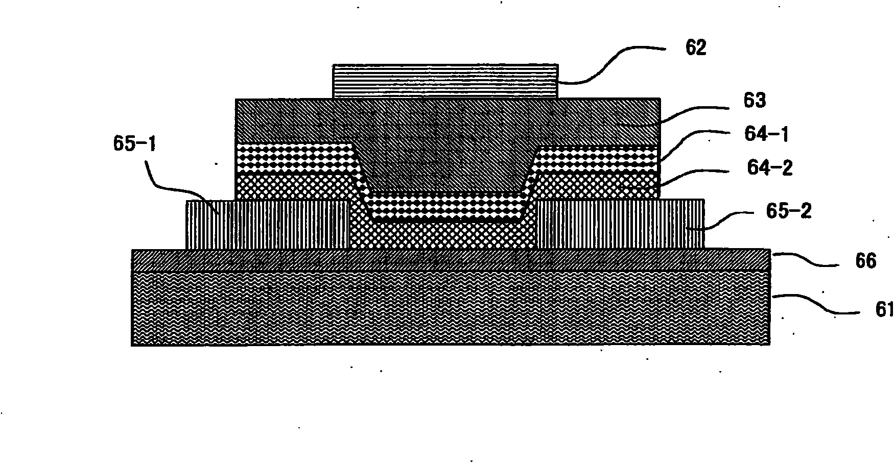
Embodiment 3
PUM
 Abstract
Description
Claims
Application Information