

Optical arrangement for assay reading device
A technology for reading devices and analyzing results, used in analyzing materials, measuring devices, and analyzing materials by optical means.
- Summary
- Abstract
- Description
- Claims
- Application Information
AI Technical Summary
Problems solved by technology
Method used
Image

Examples
Embodiment 1
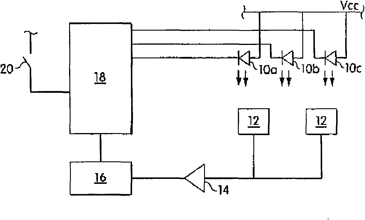
[0041] figure 1 The explanation explains an embodiment of the analysis result reading device that includes both a shared light detector and a "common reading" area.
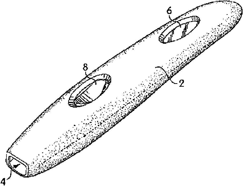
[0042] The reading device is about 12 cm long and about 2 cm wide, and is basically shaped like a finger or a cigarette. In a preferred embodiment, the length of the housing does not exceed about 12 cm, the width does not exceed about 2.5 cm, and the height does not exceed about 2.2 cm. However, any suitable shape can be adopted, such as a credit card-shaped reader. The device consists of opaque synthetic plastics (such as polycarbonate, acrylonitrile-butadiene-styrene, polystyrene, high-density polyethylene, or polypropylene or polystyrene containing appropriate light-shielding pigments such as carbon) Manufactured shell 2. There is a slit or hole 4 at one end of the reading device from which a test strip (not shown) can be inserted into the reader.
[0043] There are two oval holes on the upper surface of the rea...
Embodiment 2
[0056] This embodiment describes in more detail the features of the preferred configuration of the light emitting diode and photodiode outlined in Embodiment 1.
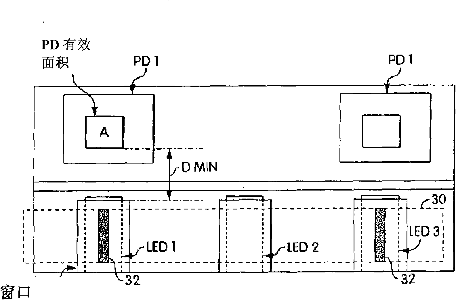
[0057] image 3 A plan view of a specific embodiment of the optical device is shown. In this embodiment, the optical device includes three light emitting diodes and two light detectors. The effective area (A) of the photodetector (PD) is 1.5mm×1.5mm. The optical elements are arranged such that the axes of the light emitting diodes 1 and 3 correspond to the axes of PD1 and PD2. The three light-emitting diodes and the two light detectors are arranged in an area of approximately no more than 1 square centimeter, preferably no more than approximately 0.7 square centimeters, especially 1 cm×0.7 cm.
[0058] At the same time, the position of the test strip 30 is shown, which is located above the light emitting diode. Insert the test strip so that the test and control lines 32 are located above the corresponding LEDs 1 and ...
Embodiment 3
[0069] In a specific embodiment, the effective area of the light detector is 2 mm×2 mm. The light source provides light, and at least part of the light has a wavelength of 635 nm. The test strip is 5.5mm higher than the light source. The height of the wall separating the LEDs is 2.7 mm and the inclination angle of the wall is 30 degrees. The plastic used is black nylon.
PUM
| Property | Measurement | Unit |
|---|---|---|
| length | aaaaa | aaaaa |
| width | aaaaa | aaaaa |
| height | aaaaa | aaaaa |
Abstract
Description
Claims
Application Information