Method for preparing crystalline silicon solar battery electrode by utilizing overprinting way

A technology for preparing solar cells and electrodes, applied in circuits, electrical components, semiconductor devices, etc., can solve problems such as electrical conductance and electrode contact, and achieve the effects of improving fill factor, avoiding disconnection, and good electrical conductance

Inactive Publication Date: 2010-02-24
CHINA SUNERGY CO LTD
View PDF0 Cites 22 Cited by
  • Summary
  • Abstract
  • Description
  • Claims
  • Application Information

AI Technical Summary

Problems solved by technology

[0006] The technical problem to be solved by the present invention is to overcome the defects existing in the prior art, and provide a method for preparing electrodes of crystalline silicon solar cells by overprinting, and solve the problems of electrode contact and conduction by two or more printings

Method used


Image

  • Method for preparing crystalline silicon solar battery electrode by utilizing overprinting way
  • Method for preparing crystalline silicon solar battery electrode by utilizing overprinting way
  • Method for preparing crystalline silicon solar battery electrode by utilizing overprinting way

Examples


Embodiment 1

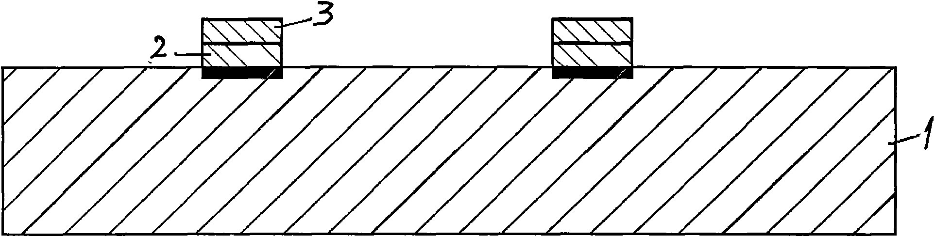
[0023] Embodiment 1, completely symmetrical overprinting, overprinting patterns coincide, and its process steps are as follows:

[0024] 1. Put the semi-finished silicon wafer to be prepared on the printing table, and use aluminum paste to do the first electrode printing according to the printing pattern designed for contact. Then the silicon wafer is dried or sintered.

[0025] 2. Then use silver paste for the above-mentioned silicon chip to do the second electrode printing according to the printing pattern in step 1, completely cover and overprint on the first electrode printing pattern. The silicon wafer is dried or sintered.

[0026] The side cross-sectional structure of the silicon wafer and the electrode after the electrode printing is completed is as follows: figure 1 shown.

Embodiment 2

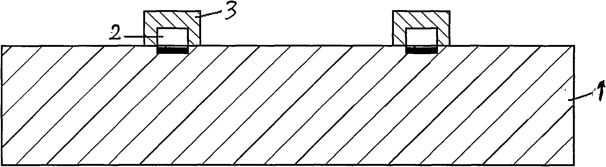
[0027] Embodiment 2, non-completely symmetrical overprinting, its process step is as follows:

[0028] 1. Put the semi-finished silicon wafer to be prepared on the printing table, and use silver paste to do the first electrode printing according to the printing pattern designed for contact. The silicon wafer is dried or sintered.

[0029] 2. Then use silver paste for the above-mentioned silicon chip to do the second electrode printing according to the same printing pattern as step 1 but the pattern range is slightly larger (or slightly smaller), covering and overprinting on the first electrode printing pattern. The silicon wafer is dried or sintered.

[0030] The side cross-sectional structure of the silicon wafer and the electrode after the electrode printing is completed is as follows: figure 2 shown.

Embodiment 3

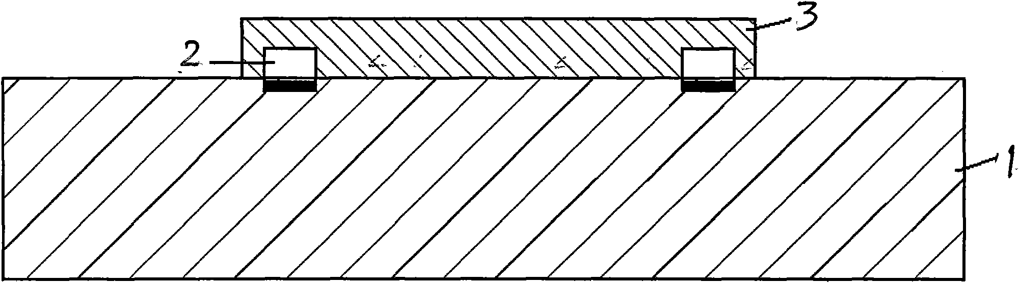
[0031] Embodiment 3, complete asymmetric overprinting, its process steps are as follows:

[0032] 1. Put the semi-finished silicon wafer to prepare the electrode on the printing table, and do the first electrode printing according to the printing pattern designed for contact. The silicon wafer is dried or sintered.

[0033] 2. Then do the second electrode printing on the above-mentioned silicon wafer according to the printing pattern designed for the battery conductive resistance, overprint on the first electrode printing pattern, and connect the electrode contact parts obtained by the first electrode printing to form a complete conduction structure. The silicon wafer is dried or sintered.

[0034] The side cross-sectional structure of the silicon wafer and the electrode after the electrode printing is completed is as follows: image 3 shown.

[0035] can be as Figure 4 as shown,

[0036] 1. You can choose aluminum paste, silver paste and other pastes with good penetrab...


PUM


Abstract

The invention discloses a method for preparing a crystalline silicon solar battery electrode by utilizing an overprinting way. The processing steps are as follows: A, preparing silicon slice for manufacturing electrodes, carrying out first electrode printing according to printing graphic aiming at contact design, and then drying and sintering; B, carrying out second electrode printing according tothe printing image of the first electrode printing or the printing image designed aiming at battery conductive resistance, overprinting on the first print graphic, and then drying and sintering. In the method of the invention, as subsequent overprinting can adopt sizing agents with different material ingredients, electrical conduction is improved, the method after whole sintering not only meets metal contact but also obtains good electrical conduction, thereby being capable of effectively improving filling factor and finally impacting on battery performance. Subsequent overprinting is attached on the surface of the first printing electrode to form a conductive structure. Overprinting process can effectively avoid frequent disconnection and incomplete printing occasions in existing printing.

Description

technical field [0001] The invention relates to a method for preparing electrodes of crystalline silicon solar cells by using the same or different patterns and the same or different pastes to print twice or more times on crystalline silicon solar cells. Background technique [0002] Nowadays, the basic process of solar cells is to print silver paste on the front, and print silver-aluminum paste and aluminum paste on the back. Loss of battery performance. [0003] For general solar cells, the general printing method is used to obtain the electrode contact, and there are certain requirements for the pattern printed on the electrode, the width and height of the grid line, and due to the limitation of the process, there are often phenomena such as disconnection and incomplete printing, which are greatly affected. affect the final performance of the battery. [0004] For high-efficiency solar cells, the process has changed a lot. For a specific contact part, it is often diffic...

Claims


Application Information

Patent Timeline
Patent Type & Authority Applications(China)
IPC IPC(8): H01L31/18H01L31/0224
CPCY02P70/50
Inventor 解柔强姚文杰王建波黄海冰向妮倪志春赵建华王艾华
Owner CHINA SUNERGY CO LTD
Why Eureka
Try Eureka