Method and device for detecting precision wafer based on parallel optical flat splitting polarized beam and phase-shifting interferometry

A parallel flat crystal, phase-shift interference technology, applied in measurement devices, optical devices, analysis of materials, etc., can solve the problems of large system error, easy to be affected by external interference, low measurement accuracy, etc., to achieve low system error and simplified optical path. The effect of high design and measurement accuracy

Inactive Publication Date: 2010-03-10
HARBIN INST OF TECH SHENZHEN GRADUATE SCHOOL
View PDF0 Cites 12 Cited by
  • Summary
  • Abstract
  • Description
  • Claims
  • Application Information

AI Technical Summary

Problems solved by technology

However, the existing phase-shift interferometry measurement methods usually measure the surface topography at points, and are easil

Method used


Image

  • Method and device for detecting precision wafer based on parallel optical flat splitting polarized beam and phase-shifting interferometry
  • Method and device for detecting precision wafer based on parallel optical flat splitting polarized beam and phase-shifting interferometry
  • Method and device for detecting precision wafer based on parallel optical flat splitting polarized beam and phase-shifting interferometry

Examples


Embodiment Construction

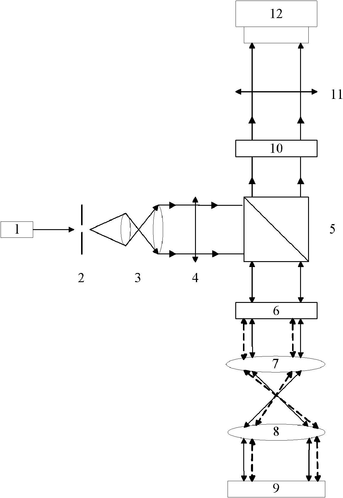
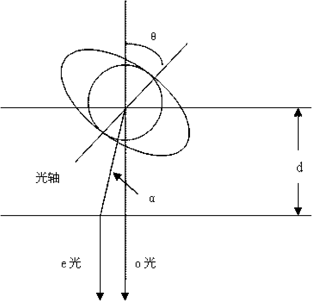
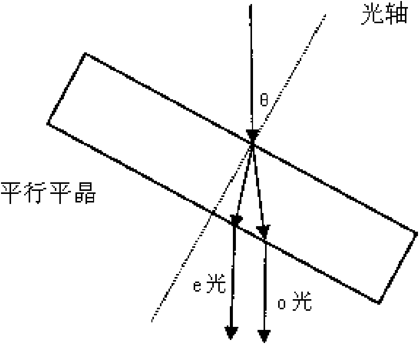
[0018] see figure 1 , is a structural schematic diagram of the optical path system of a preferred embodiment of a precision wafer inspection device based on parallel planar split-polarized beams and phase-shift interferometry according to the present invention. The detection device includes a light source 1, a spatial filter 2, a beam expander 3, a polarizer 4, a depolarization beam splitter prism 5, a parallel flat crystal 6, a first convex lens 7, a second convex lens 8, and a 1 / 4 wave plate 10. Analyzer 11 and CCD imaging device 12. figure 1 The surface 9 of the measured object is also indicated in .

[0019] The light source 1, the spatial filter 2, the beam expander 3, and the polarizer 4 are arranged in sequence. The depolarization beam splitting prism 5, the parallel flat crystal 6, the first convex lens 7, the second convex lens 8 and the surface 9 of the measured object are arranged in sequence. The depolarizing beam splitting prism 5, 1 / 4 wave plate 10, analyzer 1...


PUM


Abstract

The invention relates to a device for detecting a precision wafer based on parallel optical flat splitting polarized beam and phase-shifting interferometry. The device comprises a light source, a spatial filter, a beam expander, a polarizer, a depolarizing dispersion prism, a parallel optical flat, a quarter-wave plate and an analyzer, wherein the light source, the spatial filter, the beam expander and the polarizer are arranged on a first optical axle in sequence, the analyzer, the quarter-wave plate, the depolarizing dispersion prism, the parallel optical flat and the surface of an externalobject to be measured are arranged on a second optical axle in sequence, and the first optical axle is perpendicular to the second optical axle.

Description

technical field [0001] The invention relates to a detection method and device using polarized light interferometry technology, in particular to a precision wafer detection method and device based on parallel planar split polarized light beams and phase-shift interferometry. Background technique [0002] Surface topography measurement plays a great role in the automatic inspection of industrial products, machinery manufacturing, electronics industry, robot vision and other fields. The measurement of ultra-fine surface microtopography with a longitudinal resolution of nanometer or subnanometer has great application value in the fields of microfabrication, binary optics, X-ray optics, and biomedicine. In addition, the surface micro-profile testing technology is also of great significance and broad application prospects in the fields of robot vision, physical simulation, and computer-aided design. [0003] The combination of surface topography measurement technology and modern ...

Claims


Application Information

Patent Timeline
IPC IPC(8): G01B11/24G01N13/00
Inventor 姚勇宋菲孙云旭安宏宇
Owner HARBIN INST OF TECH SHENZHEN GRADUATE SCHOOL
Why Eureka
Try Eureka