Charge pump output voltage regulation circuit

A technology for output voltage and circuit regulation, applied in the direction of regulation of electrical variables, control/regulation systems, instruments, etc., can solve problems such as complex circuit structure, unstable charge pump output voltage, circuit characteristic changes, etc.

Inactive Publication Date: 2010-03-17
SEMICON MFG INT (SHANGHAI) CORP
View PDF0 Cites 34 Cited by
  • Summary
  • Abstract
  • Description
  • Claims
  • Application Information

AI Technical Summary

Problems solved by technology

[0005] Although the above prior art realizes the adjustment of the output voltage, it needs to use a discharge circuit or an additional reference voltage generating circuit, and the circuit structure is complicated and increases the area of ​​the chip.
Moreover, the introduction of these analog circuits will produce the phenomenon that the circuit characteristics change with the process and temperature. This unstable factor also brings challenges to the accuracy of the charge pump output voltage.

Method used


Image

  • Charge pump output voltage regulation circuit
  • Charge pump output voltage regulation circuit
  • Charge pump output voltage regulation circuit

Examples


Embodiment Construction

[0019] In order to make the technical features of the present invention more comprehensible, the present invention will be further described below in conjunction with the accompanying drawings and embodiments.

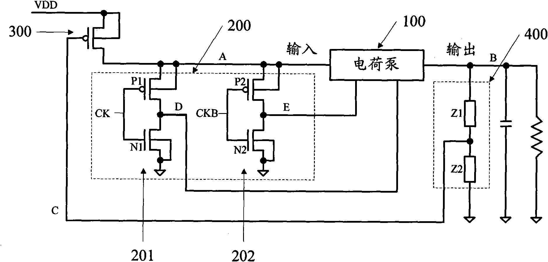
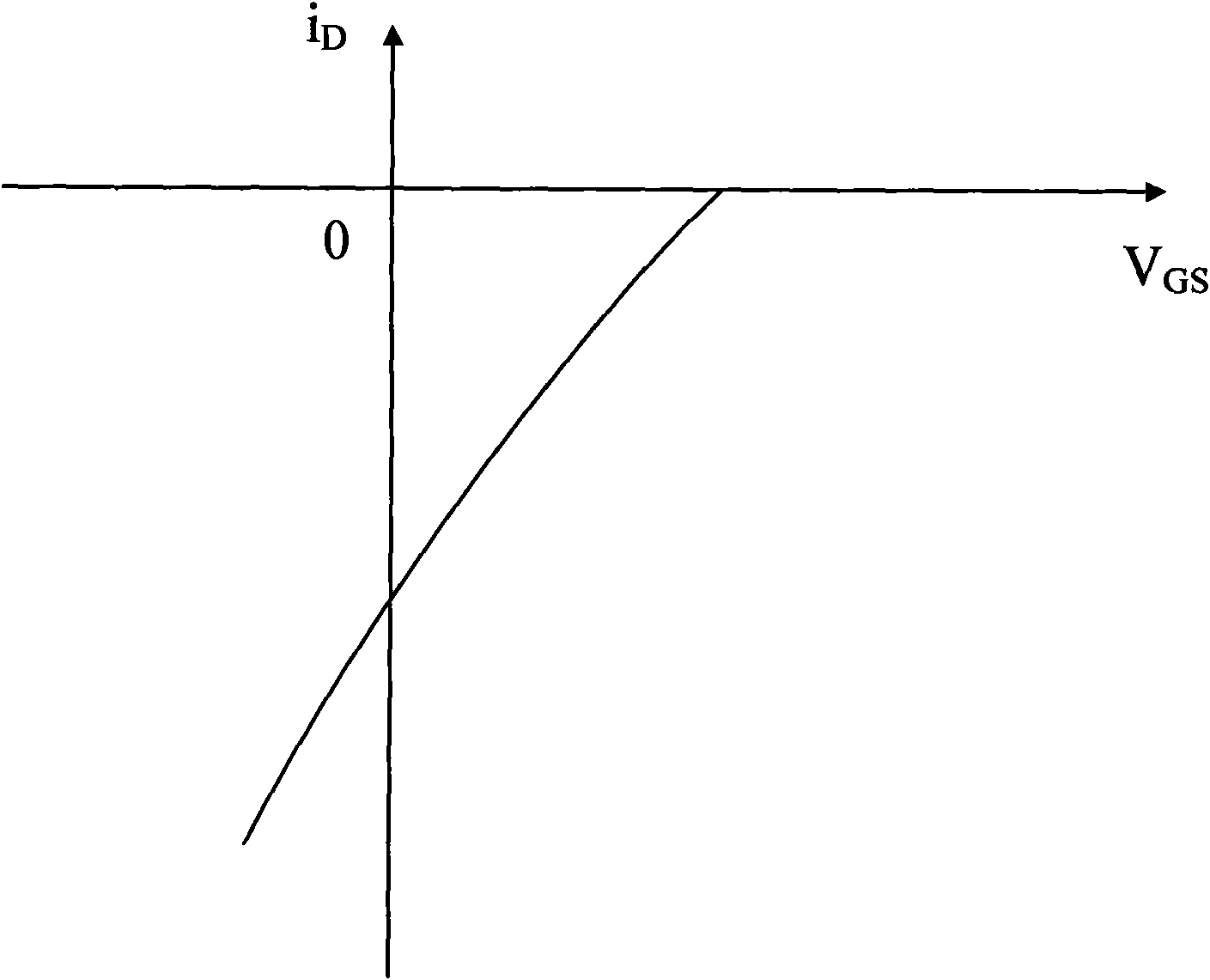
[0020] The following embodiments utilize the characteristics that the on-resistance of a P-channel Metal-Oxide-Semiconductor Field Effect (PMOS) transistor varies with the gate voltage, especially the conduction characteristics of the PMOS transistor (that is, the source is coupled to the driving voltage, the gate is connected to the When the potential difference of the source is less than a certain value, the PMOS transistor is turned on) to control the input voltage of the charge pump and the amplitude of the clock signal, thereby realizing the adjustment of the output voltage.

[0021] Please refer to figure 2 , which is a charge pump output voltage regulating circuit provided by an embodiment of the present invention, which regulates the output voltage of the char...


PUM


Abstract

The invention discloses a charge pump output voltage regulation circuit, which regulates the output voltage of a charge pump so as to generate a required stable voltage value. The voltage regulation circuit comprises a CMOS phase inverter unit and a PMOS transistor, wherein the CMOS phase inverter unit receives a clock input signal from the charge pump and feeds the inverted clock input signal back to the charge pump; and a source electrode of the PMOS transistor is coupled with the input voltage of the charge pump, a grid electrode of the PMOS transistor is coupled with a feedback signal of the output voltage of the charge pump, and a drain electrode of the PMOS transistor is connected with the power input end of the charge pump and the CMOS phase inverter unit. The mode reduces the introduction of an additional analog circuit, reduces the complexity of the circuit and improves the stability of the circuit.

Description

technical field [0001] The invention relates to the field of charge pumps, in particular to a charge pump output voltage regulation circuit. Background technique [0002] A charge pump is a capacitive voltage converter that can be used to step up or down a voltage, or to generate a negative voltage. Because of its simple circuit and high efficiency, it is widely used in integrated circuits powered by a single power supply. For example, in Electrically Erasable Programmable Read-Only Memory (EEPROM) or Flash Memory (Flash Memory), the charge pump converts the power supply voltage into a high voltage signal higher than the power supply voltage to drive the write operation of the load, PROM or FlashEPROM. [0003] However, the output voltage generated by the charge pump without any restrictions often deviates from the required value, so the voltage regulation circuit is often set to clamp its output voltage at the required value, and at the same time, the charge pump has A ce...

Claims


Application Information

Patent Timeline
Patent Type & Authority Applications(China)
IPC IPC(8): H02M3/07G05F1/56
Inventor 李明王阳元
Owner SEMICON MFG INT (SHANGHAI) CORP
Why Eureka
Try Eureka