
Method for manufacturing gan-based nitride semiconductor self-supporting substrate

A nitride semiconductor and manufacturing method technology, which is applied in the fields of semiconductor/solid-state device manufacturing, semiconductor devices, chemical instruments and methods, etc., can solve the problems of low yield, difficulty in manufacturing large-size self-supporting substrates, and high price

Inactive Publication Date: 2010-03-24
エーイーテック
View PDF5 Cites 7 Cited by
  • Summary
  • Abstract
  • Description
  • Claims
  • Application Information

AI Technical Summary

Problems solved by technology

[0011] Laser lift-off technology is a technology that separates substrates by absorbing laser light from the interface under high-power laser irradiation, but it is difficult to produce large-sized self-supporting substrates
In addition, the VAS technology is based on the phenomenon of natural exfoliation, but requires complex processes such as the preparation of GaN templates and the evaporation of metal layers.
[0012] In addition, there is a method of growing thick-film GaN on a GaAs substrate and removing the GaAs substrate by chemical etching. However, in high-temperature growth, there are problems such as decomposition of the GaAs substrate and interdiffusion at the interface, and special growth techniques are required.
Due to the complexity of such a production process and problems with yield, it has not been widely used
[0013] In summary, existing GaN-based self-supporting substrates have major problems of low yield and high cost due to complicated processes

Method used


Image

  • Method for manufacturing gan-based nitride semiconductor self-supporting substrate
  • Method for manufacturing gan-based nitride semiconductor self-supporting substrate
  • Method for manufacturing gan-based nitride semiconductor self-supporting substrate

Examples


Embodiment Construction

[0048] In the present invention, a method for producing a GaN self-supporting substrate using the HVPE method is given as an example.

[0049] This embodiment uses the following steps 1) to 5) as basic steps.

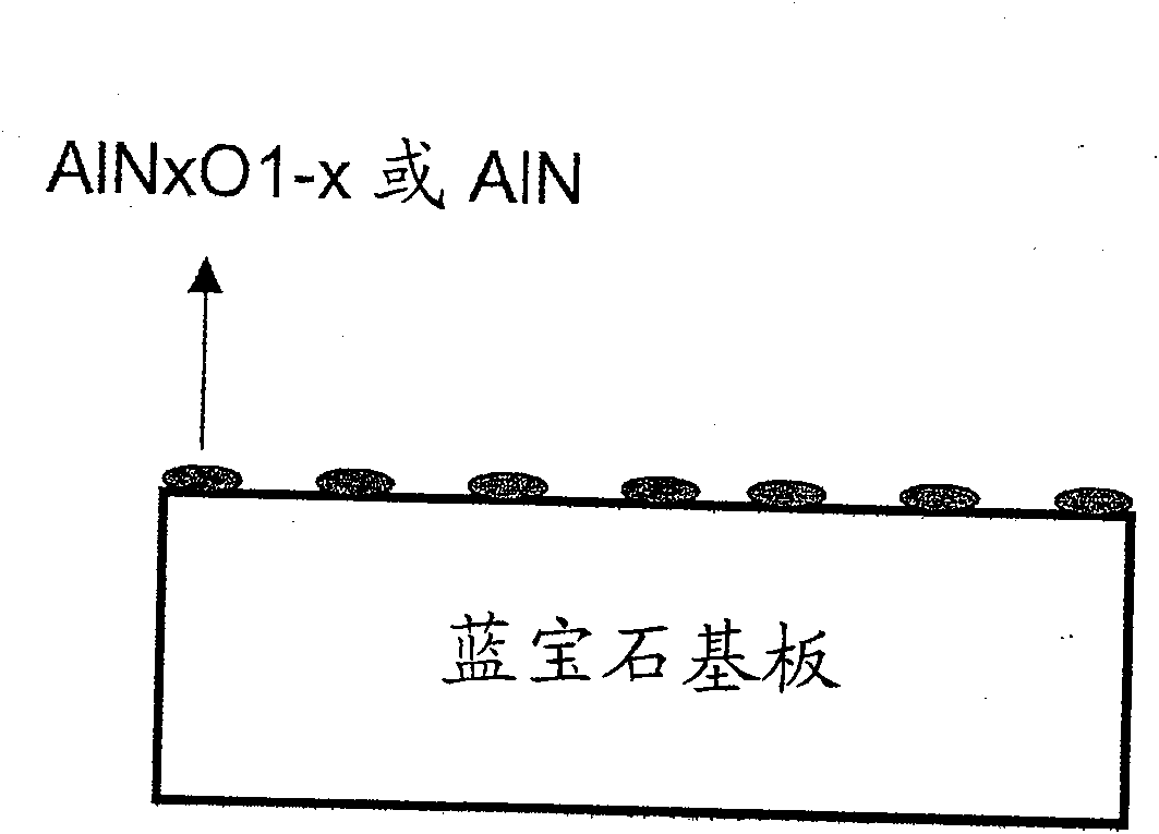
[0050] 1) High temperature nitriding process of sapphire substrate

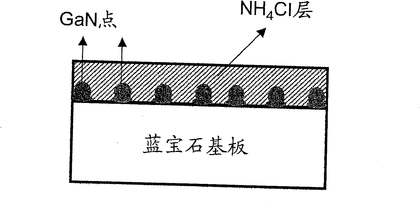
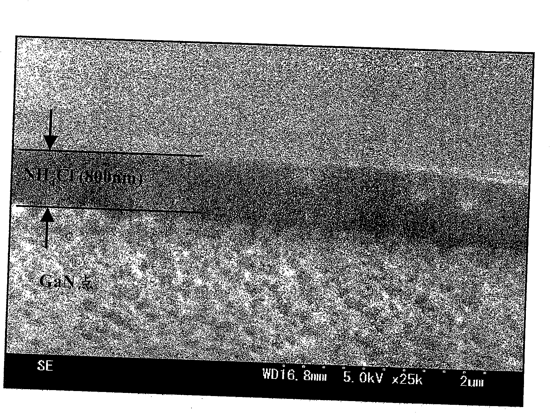
[0051] 2) NH 4 Cl layer and GaN dot formation process

[0052] 3) Growth process of low temperature GaN buffer layer

[0053] 4) Formation process of high-temperature thick-film GaN layer

[0054] 5) Self-stripping process of GaN self-supporting substrate

[0055] Furthermore, in this example, a c-plane grown GaN self-supporting substrate was obtained through steps 1) to 5).

[0056] The above steps 1) to 5) will be described in detail below.

[0057] 1) High temperature nitriding process of sapphire substrate

[0058] This process is to locally form AlN on the surface of the sapphire substrate through high-temperature nitriding treatment of the sapphire substrate in the HVPE reactor X o 1-X (0<...


PUM

PropertyMeasurementUnit
Thicknessaaaaaaaaaa
Diameteraaaaaaaaaa
Boiling pointaaaaaaaaaa

Abstract

To provide a method for manufacturing a stress-free GaN-based nitride compound semiconductor at low cost by simple process. [MEANS FOR SOLVING PROBLEMS] A method for manufacturing a GaN-based nitride semiconductor self-supporting substrate includes a step of preparing a substrate; a step of forming a GaN dot and an NH4Cl layer on the substrate; a step of forming a low-temperature GaN buffer layeron the GaN dot and the NH4Cl layer; a step of forming a GaN nitride semiconductor layer on the low-temperature GaN buffer layer; and a step of naturally removing the GaN-based nitride semiconductor layer from the substrate by returning the substrate temperature to a normal temperature.

Description

technical field [0001] The present invention relates to a method for manufacturing a GaN-based nitride semiconductor self-supporting substrate. Background technique [0002] In order to realize blue and ultraviolet high-power laser diodes, high-brightness LEDs, and high-power electronic devices, components based on nitride semiconductors are developing toward higher performance. Currently, in the production of GaN-based optical or electronic devices, sapphire substrates are mainly used as substrates for crystal growth. [0003] However, in the case of using a sapphire substrate, the dislocation density (dislocation density) is 10 due to the large lattice mismatch between the substrate and the GaN-based nitride semiconductor and the difference in thermal expansion coefficient. 10 / cm 2 about. Also, there are problems such as degradation of element characteristics due to such a large defect density. [0004] In order to reduce the dislocation density, a variety of buffer l...

Claims


Application Information

Patent Timeline
IPC IPC(8): C30B29/38C30B25/18H01L33/12H01L33/32
CPCC30B25/16C30B25/165C30B25/18C30B29/38H01L21/20
Inventor 八百隆文曹明焕
Owner エーイーテック
Learn More