Method for selectively depositing diffusion barrier for copper interconnection

A technology for depositing copper and barrier layers, which is applied in the direction of electrical components, semiconductor/solid-state device manufacturing, circuits, etc., can solve the problems of increasing circuit RC interconnection delay, contact resistance and interconnection resistance increase, etc.

Inactive Publication Date: 2010-04-07
FUDAN UNIV
View PDF0 Cites 13 Cited by
  • Summary
  • Abstract
  • Description
  • Claims
  • Application Information

AI Technical Summary

Problems solved by technology

As the integrated circuit technology node moves to a process below 45nm, the size of the through-hole in the back-end interconnection technology becomes smaller and smaller. The diffusion barrier layer grown at the bottom of the through-hole and the two interfaces of the copper wire and the copper through-hole, And the diffusion barrier layer itself accounts for a large proportion of the resistance of the entire via, so the contact resistance and interconnect resistance will increase accordingly, increasing the RC interconnect delay of the circuit

Method used


Image

  • Method for selectively depositing diffusion barrier for copper interconnection
  • Method for selectively depositing diffusion barrier for copper interconnection
  • Method for selectively depositing diffusion barrier for copper interconnection

Examples


Embodiment Construction

[0027] Below in conjunction with accompanying drawing and specific embodiment the present invention is described in further detail:

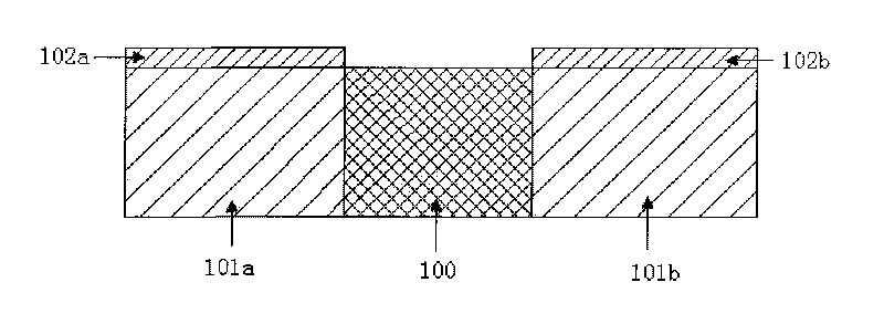
[0028] Step 1: Please refer to figure 1 , providing an integrated circuit substrate in which a certain level of wiring of an interconnection structure has been completed, the material 100 is copper, the materials 101a and 101b are low dielectric constant dielectrics, and the materials 102a and 102b are silicon nitride or other etching barrier materials .

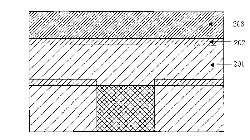
[0029] Step 2: Please refer to figure 2 A thin film 201, a thin film 202 and a thin film 203 are sequentially formed on the provided substrate, the thin film 201 is a low dielectric constant medium, the thin film 202 is silicon nitride or other etching barrier materials, and the thin film 203 is a photoresist layer.

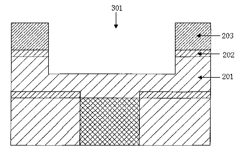
[0030] Step 3: Please refer to image 3 , after determining the position of the interconnect groove, an opening 301 is formed in the film 203 , the film 202 and the film 201 ...


PUM

PropertyMeasurementUnit
electrical resistivityaaaaaaaaaa

Abstract

The invention belongs to the technical field of integrated circuits and particularly discloses a method for selectively depositing a diffusion barrier for copper interconnection, which comprises a step of before depositing the diffusion barrier, coating a layer of organic group on an exposed copper surface to prevent the absorption of a precursor on the copper surface in an atomic layer depositing process to selectively deposit the diffusion barrier. In the method, the deposition of the diffusion barrier in places except for the bottom of a copper interconnection hole is realized, so the unnecessary diffusion barrier in the copper through hole is removed and the contact resistance in the through hole is reduced. Thus, the resistance of the system is reduced and consequentially the RC delay of the whole circuit is reduced.

Description

technical field [0001] The invention belongs to the technical field of large-scale integrated circuits and relates to a technology for depositing a diffusion barrier layer, in particular to a method for selectively depositing a diffusion barrier layer for copper interconnection. Background technique [0002] With the continuous advancement of VLSI process technology, the feature size of semiconductor devices is getting smaller and smaller, and the integration level is getting higher and higher. The thinner metal wires designed in VLSI will increase the metal resistance and generate more heat. , resulting in serious electromigration phenomenon, and at the same time, the delay (RCDelay) caused by the increase of inter-line capacitance and metal resistance is also deteriorating, which greatly affects the performance of semiconductor chips. [0003] Compared with conventional aluminum, copper has the following advantages: First, the resistivity of copper is smaller (Cu: 1.7 μΩ / c...

Claims


Application Information

Patent Timeline
Patent Type & Authority Applications(China)
IPC IPC(8): H01L21/768
Inventor 孙清清王鹏飞丁士进张卫
Owner FUDAN UNIV
Why Eureka
Try Eureka