Free-etching oxidation manufacturing method of SOI submicron ridge optical waveguide back-taper coupler

A manufacturing method and optical waveguide technology, applied in the field of integrated optoelectronics, to achieve the effect of smooth side walls of the waveguide and low scattering loss

Inactive Publication Date: 2010-05-19
INST OF SEMICONDUCTORS - CHINESE ACAD OF SCI
View PDF0 Cites 16 Cited by
  • Summary
  • Abstract
  • Description
  • Claims
  • Application Information

AI Technical Summary

Problems solved by technology

Therefore, the key to making the inverted cone coupler integrated with the ridge optical waveguide is to solve the unb

Method used


Image

  • Free-etching oxidation manufacturing method of SOI submicron ridge optical waveguide back-taper coupler
  • Free-etching oxidation manufacturing method of SOI submicron ridge optical waveguide back-taper coupler
  • Free-etching oxidation manufacturing method of SOI submicron ridge optical waveguide back-taper coupler

Examples


Embodiment Construction

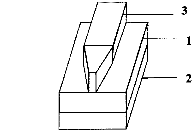
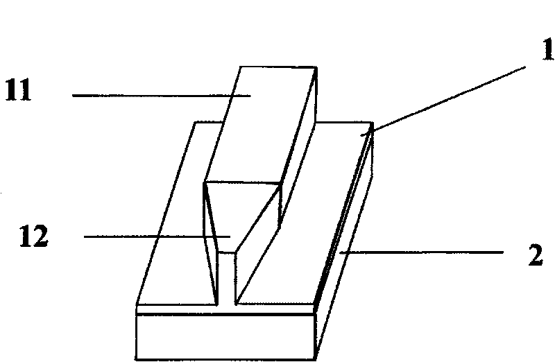
[0029] see Figure 1 to Figure 8 As shown, the present invention relates to a kind of SOI submicron ridge optical waveguide inverted cone coupler free from etching and oxidation manufacturing method, comprising the following steps:

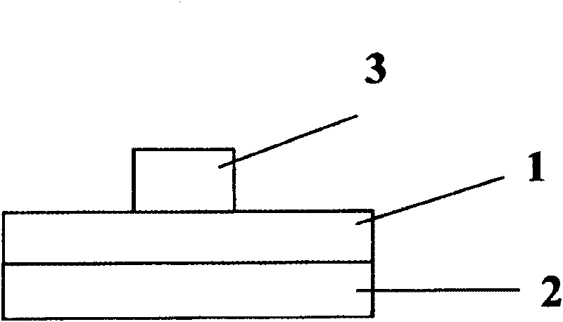
[0030] Step 1: Oxidize a layer of 500 nanometer silicon dioxide layer 1 on the top layer silicon 2 (thickness 340 nanometers) of SOI, this process actually consumes the top layer silicon 2 thickness of SOI is about 230 nanometers, and this oxide layer thickness can make The top layer silicon 2 of SOI under the silicon layer 1 can effectively resist the subsequent oxidation process.

[0031] Step 2: Form a mask pattern 3 on the silicon dioxide layer 1 through a photolithography process. One end of the mask pattern is rectangular for subsequent formation of a ridge waveguide; the other end is tapered for subsequent formation of a ridge waveguide. type waveguide integrated strip waveguide inverted cone structure.

[0032] Step 3: Etch the silicon d...


PUM

PropertyMeasurementUnit
Thicknessaaaaaaaaaa
Thicknessaaaaaaaaaa

Abstract

The invention relates to a free-etching oxidation manufacturing method of an SOI submicron ridge optical waveguide back-taper coupler, comprising the following steps: (1) oxidizing a silicon dioxide layer on SOI top-layer silicon; (2) forming a mask image on the silicon dioxide layer by a photoetching technology, wherein one end of the mask image is rectangular and the other end of the mask image is tapered by an etching technology; etching the silicon dioxide layer which is not protected by the mask image; and then forming a rectangular area and a tapered area of silicon dioxide protected by the mask image; (3) removing the mask image which is remained on the SOI top-layer silicon to form a sample; (4) oxidizing the sample, and oxidizing the etched SOI top-layer silicon under the etched silicon dioxide layer to a predetermined height so as to form a ridge waveguide flat area; (5) forming a ridge waveguide inner-ridge area on the SOI top-layer silicon protected by the tapered area of the silicon dioxide layer to form a slab waveguide back-taper structure which is connected with the inner-ridge area in a natural transition mode, and thus completing the natural integration of the ridge waveguide and the back-taper coupler.

Description

technical field [0001] The invention relates to the field of integrated optoelectronics, and provides an etching and oxidation-free manufacturing method for an SOI submicron ridge optical waveguide inverted cone coupler. Background technique [0002] In the field of optics, we often encounter the problem of optical coupling of optical waveguides with different cross-sectional sizes. When the light of the waveguide is coupled into a large-sized optical waveguide, a large optical loss will be caused. [0003] There is also the coupling problem between optical waveguides of different structures. The general shape of the ridge-type optical waveguide is like a "convex" shape, and the raised middle area is the main light-guiding area, which is called the inner ridge area or ridge-type area, and the two sides of the ridge-type area are open and extended, and the light transmitted between them Rarely, it is called a flat zone. The advantage of this structure is that it greatly re...

Claims


Application Information

Patent Timeline
IPC IPC(8): G02B6/13
Inventor 陈少武程勇鹏任光辉樊中朝
Owner INST OF SEMICONDUCTORS - CHINESE ACAD OF SCI
Why Eureka
Try Eureka