Slow wave structure based on semiconductor-filled metal waveguide structure

A slow-wave structure and metal-filled technology, applied in the field of slow-wave structures, can solve the problems of increasing electromagnetic wave scattering loss, difficulty in the preparation of slow-wave devices, and difficulty in preparation, achieving good loss characteristics, easy design and processing, and solving the problem of preparation. difficult effect

Inactive Publication Date: 2011-09-14
CHINA JILIANG UNIV
View PDF2 Cites 7 Cited by
  • Summary
  • Abstract
  • Description
  • Claims
  • Application Information

AI Technical Summary

Problems solved by technology

Most of these slow-wave structures need to introduce fine periodic structures or resonant cavity structures, which brings difficulties to the preparation of slow-wave devices (especially high-frequency electromagnetic wave devices), and the gaps and process errors of periodic structures will increase the impact on electromagnetic waves. Scattering loss, and difficult to couple
Although the slow-wave waveguide structure composed of artificial composite electromagnetic media such as left-handed media no longer needs a periodic structure and a resonant cavity structure, the medium itself is a periodic composite structure, which is extremely difficult to prepare and has a large loss for slow waves. Such a structure with ideal slow-wave properties is difficult to practically prepare

Method used


Image

  • Slow wave structure based on semiconductor-filled metal waveguide structure
  • Slow wave structure based on semiconductor-filled metal waveguide structure
  • Slow wave structure based on semiconductor-filled metal waveguide structure

Examples


Embodiment 1

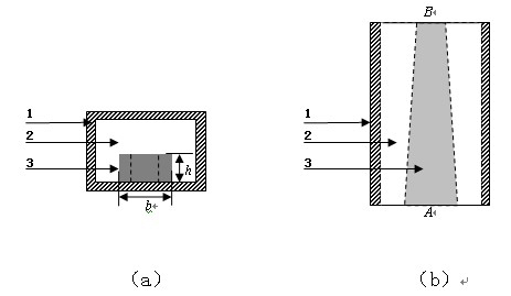
[0029] refer to figure 1 , a slow-wave waveguide based on a semiconductor-filled metal waveguide structure, comprising a rectangular metal waveguide wall 1 , a tapered semiconductor dielectric quadrangular prism 3 and air 2 . The length and width of the metal waveguide section are 80 and 40 . Height of pyramid-shaped semiconductor dielectric h Constant along the longitudinal direction, it is 16 , only the width b It becomes smaller along the longitudinal direction, and its material is germanium. Where A is the incident port of the electromagnetic wave. The present invention is a gradually tapered waveguide structure with the same structural parameters in the waveguide direction, rather than a periodic structure, and the structure of the present invention is much simpler than other slow wave structures.

[0030] In this embodiment, when the electromagnetic wave propagates along the waveguide structure, the energy flow transmitted in the air gap layer gradually increas...

Embodiment 2

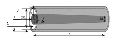
[0032] refer to image 3 , a slow-wave structure based on a semiconductor-filled metal waveguide structure, including a circular metal waveguide wall 1, air 2 and a tapered gallium arsenide semiconductor strip 3. The radius of GaAs semiconductor dielectric changes from the longitudinal direction, R 1 =0.23mm,R 2 =0.21mm,L=12mm,R 0 =0.4mm.

[0033] Electromagnetic waves flow from the wide port of the semiconductor A incident, propagates along the waveguide. Since the semiconductor near the port is wider, the guided wave has a larger group velocity. With the propagation of the guided wave, the average energy flow in the air is gradually close to the value in the semiconductor, the group velocity of the guided wave is gradually reduced, and the energy of the electromagnetic wave is gradually concentrated and strengthened. The corresponding part of the waveguide increases to the strongest, and electromagnetic waves of different frequencies will be enhanced in different parts ...


PUM


Abstract

The invention discloses a slow wave structure based on a semiconductor-filled metal waveguide structure. The slow wave structure comprises a uniform metal hollow waveguide pipe wall, an air gap and a conical filled high-refractive index semiconductor medium strip. In the slow wave structure, by utilizing the abnormal characteristic that the direction of energy flow in the air gap is opposite to that of energy flow in media when electromagnetic waves are transmitted in a high-refractive index semiconductor-filled waveguide structure and selecting parameters of the waveguide structure reasonably, the average energy flow of the electromagnetic waves with different frequencies in air and the average energy flow of the electromagnetic waves with different frequencies in a semiconductor at the corresponding position of waveguide are approximate, so the electromagnetic waves have extremely low group velocity. When the electromagnetic waves enter a port and are transmitted along the waveguide, the group velocity of the electromagnetic waves is reduced gradually, and the energy of the electromagnetic waves is enhanced gradually until the electromagnetic waves reach specific parts corresponding to the frequencies; and waveguide parts in which the electromagnetic waves with the different frequencies can reach are different from one another, so the frequency division, field restriction and reinforcing effects of the electromagnetic waves are realized simultaneously by the structure.

Description

technical field [0001] The invention relates to the fields of physical electronic devices and terahertz wave devices, in particular to a slow-wave structure in devices or devices that can be used for the interaction between low-speed electromagnetic waves and electrons or other substances. Background technique [0002] Due to the slow speed of electromagnetic waves propagating in the slow wave structure, the interaction between electromagnetic waves and matter is greatly enhanced, which makes the slow wave structure play an important role in sensing, amplification, source and miniaturized devices in the field of microwave and terahertz waves. For example, the slow wave structure in the microwave field is mainly used in traveling wave amplifiers, particle accelerators and other devices. In some wedge-shaped or tapered slow-wave structures, different frequencies of the guided wave can stagnate and intensify at different parts of the structure, forming the so-called "constraine...

Claims


Application Information

Patent Timeline
Patent Type & Authority Applications(China)
IPC IPC(8): H01J23/24
Inventor 何金龙李向军汪伟洪治
Owner CHINA JILIANG UNIV
Why Eureka
Try Eureka