
Epitaxial reaction chamber cleaning method capable of improving epitaxial quality and reducing cost

A reaction chamber and epitaxy technology, applied in electrical components, semiconductor/solid-state device manufacturing, circuits, etc., can solve the problems of wafer carrier plate damage, increase epitaxy cost, increase surface particle diffusivity, etc., to improve epitaxy quality, reduce cost, the effect of improving the service life

Inactive Publication Date: 2010-05-26
GRACE SEMICON MFG CORP
View PDF0 Cites 5 Cited by
  • Summary
  • Abstract
  • Description
  • Claims
  • Application Information

AI Technical Summary

Problems solved by technology

[0008] The reason why it appears as Figure 1 to Figure 3 The reason for the stacking fault SF shown is that the wafer carrier plate is made of silicon carbide, which reacts slowly with hydrogen chloride gas at a high temperature above 1000 degrees Celsius for 30 minutes or more Prolonged hydrogen chloride gas cleaning will cause damage to the wafer carrier and increase the diffusivity of its surface particles. On the one hand, in the subsequent epitaxial process, the silicon carbide surface particles on the surface of the wafer carrier will diffuse to the wafer surface and form stacks. Stacking faults, on the other hand, will reduce the life of the wafer carrier and greatly increase the cost of epitaxy

Method used


Image

  • Epitaxial reaction chamber cleaning method capable of improving epitaxial quality and reducing cost
  • Epitaxial reaction chamber cleaning method capable of improving epitaxial quality and reducing cost
  • Epitaxial reaction chamber cleaning method capable of improving epitaxial quality and reducing cost

Examples


Embodiment Construction

[0026] The method for cleaning the epitaxial reaction chamber which can improve the epitaxial quality and reduce the cost of the present invention will be further described in detail below.

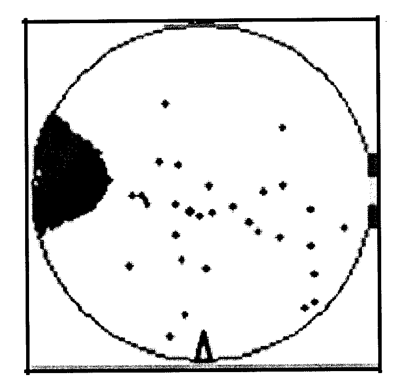
[0027] The epitaxial reaction chamber cleaning method which can improve the epitaxial quality and reduce the cost of the present invention is carried out before or after the epitaxial process. The epitaxial reaction chamber is a reaction chamber of a decompression chemical vapor deposition machine. Round carrier tray. In this embodiment, the reduced-pressure chemical vapor deposition machine is an Epi Centura epitaxy system launched by Applied Materials Inc.

[0028] The characteristics of the Epi Centura epitaxy system are: A. The wafer is set on the wafer carrier on the base and rotates with the base. By adjusting the level and height of the base, the thickness and resistance of the epitaxy grown on the wafer can be adjusted. The uniformity of the efficiency can be well guaranteed; B. ...


PUM


Abstract

The invention provides an epitaxial reaction chamber method capable of improving epitaxial quality and reducing cost. In the prior art, because an reaction chamber is subjected to hydrogen chloride gas cleaning at a high temperature of over 1,000 DEG C for 30 minutes and over 30 minutes, the diffusivity of surface granules on a wafer bearing plate is improved and the service life is reduced, so that the surface granules are diffused to epitaxy and form stacking faults on the epitaxy during epitaxial process. In the method, the reaction chamber is subjected to the hydrogen chloride gas cleaning at a high temperature of over 1,000 DEG C for 10 to 20 minutes, then the reaction chamber is regulated and controlled to be at a deposition temperature and a deposition pressure, and a gaseous silicon source is introduced, so that 20 to 100 nanometer polysilicon is deposited on the wafer bearing plate. In the method, the wafer bearing plate can be wrapped to prevent the surface granules of the wafer bearing plate from forming the stacking faults on the epitaxy so as not to influence the epitaxial quality of the epitaxial process; and in addition, the method can improve the service life of the wafer bearing plate, and reduce the cost effectively.

Description

technical field [0001] The invention relates to the field of semiconductor manufacturing, in particular to an epitaxial reaction chamber cleaning method which can improve epitaxial quality and reduce cost. Background technique [0002] The epitaxial (Epitaxy, referred to as Epi) process refers to the growth of a single crystal material with the same lattice arrangement as the substrate on a single crystal substrate. The epitaxial layer can be a homoepitaxial layer (such as Si / Si) or a Heteroepitaxial layer (eg SiGe / Si or SiC / Si, etc.). In the late 1950s, silicon epitaxial wafers were successfully used to manufacture high-frequency and high-power transistors, and showed their great advantages. After that, silicon epitaxial wafers became more and more widely used. In bipolar devices, whether they are transistors, power tubes, linear integrated circuits or digital integrated circuits, silicon epitaxial wafers are used for manufacturing. For MOS devices, although silicon epita...

Claims


Application Information

Patent Timeline
IPC IPC(8): H01L21/00
Inventor 黄锦才梅惠婷
Owner GRACE SEMICON MFG CORP
Learn More