Nitride-based semiconductor laser device and method of manufacturing the same

A technology of nitrides and laser components, which is applied in the direction of semiconductor lasers, structural details of semiconductor lasers, laser components, etc., can solve the ohmic properties of the p-side electrode layer (deterioration of contact resistance, increase of operating voltage of semiconductor laser components, etc.)

Inactive Publication Date: 2010-05-26
SANYO ELECTRIC CO LTD
View PDF1 Cites 2 Cited by
  • Summary
  • Abstract
  • Description
  • Claims
  • Application Information

AI Technical Summary

Problems solved by technology

In particular, since the degenerated layer formed in the manufacturing process deteriorates the ohmic properties (contact resistance) of the p-side electrode layer, there is a problem that the operating voltage of the semiconductor laser element increases.

Method used


Image

  • Nitride-based semiconductor laser device and method of manufacturing the same
  • Nitride-based semiconductor laser device and method of manufacturing the same
  • Nitride-based semiconductor laser device and method of manufacturing the same

Examples


Embodiment Construction

[0047] Embodiments of the present invention will be described below based on the drawings.

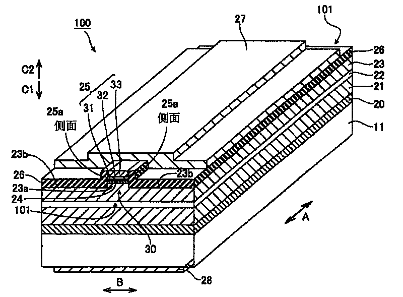
[0048] First, refer to figure 1 and figure 2 The structure of the nitride-based semiconductor laser device 100 according to one embodiment of the present invention will be described.

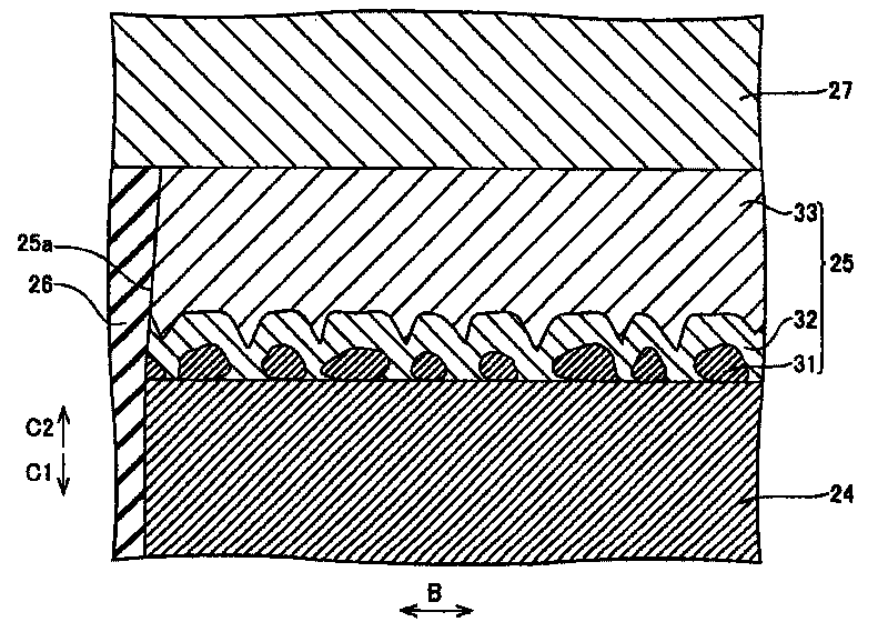
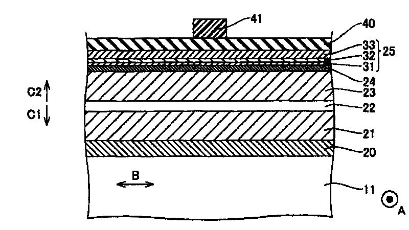
[0049] In the nitride-based semiconductor laser device 100 of the present embodiment, as figure 1 As shown, a buffer layer 20 made of AlGaN is formed on an n-type GaN substrate 11 . On the buffer layer 20, an n-type cladding layer 21 made of n-type AlGaN, a barrier layer (not shown) made of InGaN, and a well layer (not shown) made of InGaN are alternately stacked. layer 22, and a p-type cladding layer 23 made of AlInGaN and having a convex portion 23a and a flat portion 23b. A p-type contact layer 24 made of InGaN is formed on the convex portion 23 a of the p-type cladding layer 23 . In addition, the ridge 30 is formed by the convex portion 23 a of the p-type cladding layer 23 and the p-type contac...


PUM

PropertyMeasurementUnit
thicknessaaaaaaaaaa
thicknessaaaaaaaaaa
thicknessaaaaaaaaaa

Abstract

A nitride-based semiconductor laser device includes a nitride-based semiconductor layer formed on an active layer made of a nitride-based semiconductor, and an electrode layer including a first metal layer, made of Pt, formed on a far side of a surface of the nitride-based semiconductor layer from the active layer, a second metal layer, made of Pd, formed on a surface of the first metal layer, and a third metal layer, made of Pt, formed on a surface of the second metal layer, and having a shape necessary for the device in plan view. A thickness of the third metal layer is at least 10 times and not more than 30 times a thickness of the first metal layer.

Description

technical field [0001] The present invention relates to a nitride-based semiconductor laser device and a manufacturing method thereof, and more particularly to a nitride-based semiconductor laser device including a nitride-based semiconductor layer and an electrode layer and a manufacturing method thereof. Background technique [0002] In recent years, the development of nitride-based semiconductor laser devices as light sources for optical disc pickups compatible with next-generation DVDs and various display devices has been actively developed. In particular, in order to reduce the operating voltage of the nitride-based semiconductor laser device, it is required to reduce the contact resistance of electrodes formed on the semiconductor device. At this time, in the nitride-based semiconductor, since the carrier concentration of the p-type semiconductor is low, it is difficult to form a p-side electrode that obtains good ohmic properties. [0003] Therefore, currently, there...

Claims


Application Information

Patent Timeline
Patent Type & Authority Applications(China)
IPC IPC(8): H01S5/00H01S5/343H01S5/22H01S5/02
Inventor 西川学太田洁市桥由成
Owner SANYO ELECTRIC CO LTD
Why Eureka
Try Eureka